Semiconductor device and manufacturing method thereof

A manufacturing method and semiconductor technology, applied in semiconductor/solid-state device manufacturing, semiconductor devices, electrical components, etc., can solve the problems of increasing device parasitic resistance, affecting device performance, increasing source/drain parasitic resistance, and reducing parasitic resistance. , the effect of improving performance

Inactive Publication Date: 2013-02-13
INST OF MICROELECTRONICS CHINESE ACAD OF SCI
View PDF3 Cites 4 Cited by
  • Summary
  • Abstract
  • Description
  • Claims
  • Application Information

AI Technical Summary

Problems solved by technology

[0004] However, although the gate-last process of CMOSFET reduces the impact of gate oxide layer changes on device performance, it increases the source / drain parasitic resistance
refer to figure 1 , figure 1 For the COMSFET formed for the gate-last process, after the replacement gate stack 100 is formed, a contact hole is opened in the interlayer dielectric layer 110, and a metal silicide 120 is formed in the contact hole, and between the metal silicide 120 and the spacer 102 If no metal silicide is formed, it will greatly increase the parasitic resistance of the device and affect the performance of the device

Method used


Image

  • Semiconductor device and manufacturing method thereof
  • Semiconductor device and manufacturing method thereof
  • Semiconductor device and manufacturing method thereof

Examples


Embodiment Construction

[0035] In order to make the above objects, features and advantages of the present invention more comprehensible, specific implementations of the present invention will be described in detail below in conjunction with the accompanying drawings.

[0036] In the following description, a lot of specific details are set forth in order to fully understand the present invention, but the present invention can also be implemented in other ways different from those described here, and those skilled in the art can do it without departing from the meaning of the present invention. By analogy, the present invention is therefore not limited to the specific examples disclosed below.

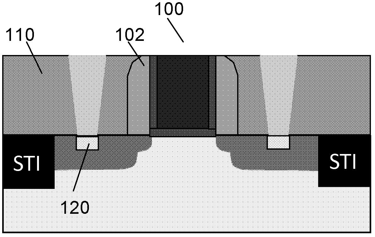
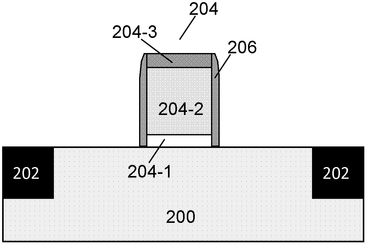
[0037] Secondly, the present invention is described in detail in combination with schematic diagrams. When describing the embodiments of the present invention in detail, for the convenience of explanation, the cross-sectional view showing the device structure will not be partially enlarged according to the gener...


PUM

PropertyMeasurementUnit
thicknessaaaaaaaaaa
thicknessaaaaaaaaaa
thicknessaaaaaaaaaa

Abstract

The invention discloses a semiconductor device and a manufacturing method thereof. The method comprises the following steps of: providing a semiconductor substrate; forming a pseudo-gate region and side walls of the pseudo-gate region on the semiconductor substrate; forming epitaxial layers on the semiconductor substrate on the two sides of the pseudo-gate region to form source and drain regions, wherein the epitaxial layers are made of metal silicide, metal germanide or metal silicon germanide; forming interlayer dielectric layers to cover the epitaxial metal silicide layers of the source and drain regions; removing the pseudo-gate region to form an opening; and forming a gate dielectric layer on the inner walls of the opening, and forming a metal gate electrode on the gate dielectric layer to fill the opening. Before a substitute gate is formed, the epitaxial layers are formed on the semiconductor substrate on the two sides of the gate region and cover the whole source and drain regions of a Schottky barrier field effect transistor device, and the height of a Schottky barrier between the epitaxial source and drain regions and a channel is effectively reduced, so that the source and drain parasitic resistance of the device is obviously reduced, and the performance of the device is improved.

Description

technical field [0001] The present invention relates to semiconductor manufacturing technology, more specifically, to a semiconductor device and its manufacturing method. Background technique [0002] With the rapid development of semiconductor technology, the feature size of semiconductor devices is shrinking continuously, which makes the integration level of integrated circuits higher and higher, which also puts forward higher requirements for the performance of devices. [0003] At present, the research on the manufacturing process of CMOSFET (Complementary Metal Oxide Semiconductor Field Effect Transistor) can be roughly divided into two directions, namely, the front gate process and the gate replacement process. Before, it will affect the gate oxide layer, and after the device size is continuously reduced, it will affect the electrical characteristics of the device, and the gate of the gate replacement process (gate last process, Gate Last) is in the source and drain F...

Claims


Application Information

Patent Timeline
Patent Type & Authority Applications(China)
IPC IPC(8): H01L21/336H01L29/78
Inventor 罗军赵超钟汇才李俊峰
Owner INST OF MICROELECTRONICS CHINESE ACAD OF SCI
Why Eureka
Try Eureka