Method of graphene manufacturing

A graphene and substrate technology, applied in the field of graphene production, can solve problems such as no sublimation or etching, uneven graphene parameters, and limited industrial applications.

Active Publication Date: 2013-02-13
INST TECH MATERIAL ELEKT
View PDF1 Cites 7 Cited by
  • Summary
  • Abstract
  • Description
  • Claims
  • Application Information

AI Technical Summary

Problems solved by technology

The disadvantages of this method include: it is difficult to obtain the equilibrium pressure of Si under vacuum conditions, which limits its industrial application; and the quality of graphene depends on the quality of the S

Method used


Image

  • Method of graphene manufacturing
  • Method of graphene manufacturing
  • Method of graphene manufacturing

Examples


Embodiment 1

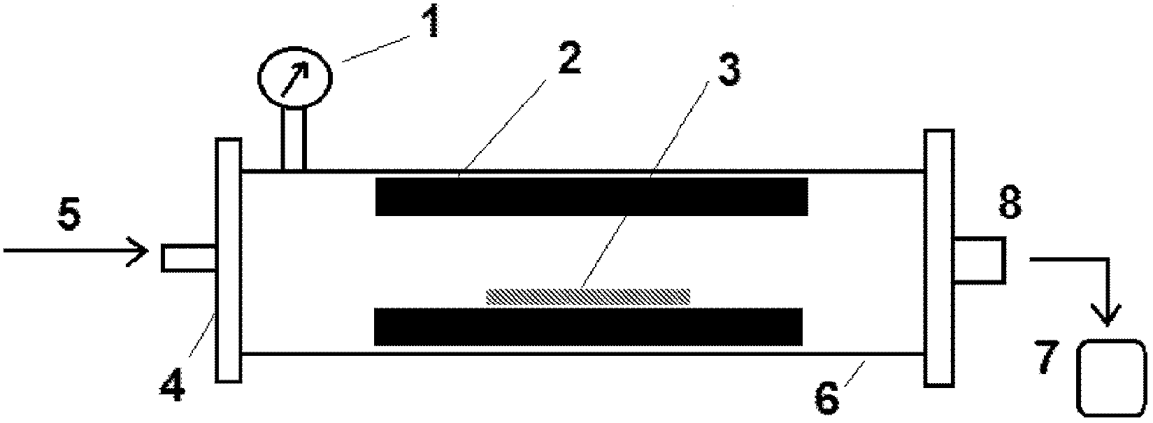
[0038] Use commercially available VP508 reactor ( figure 1 ) and a commercially available silicon carbide substrate for graphene epitaxy by CVD (Chemical Vapor Deposition), which is polytyped 4H-SiC, 6H-SiC or 3C-SiC and has an orientation (0001 ) or (000-1). Substrates with 0 to 8 degree chamfers available from manufacturers such as Cree (USA) and SiCrystal (Germany) were also used. The substrate surface (called "epi-ready") is pre-prepared by the manufacturer. Furthermore, the substrates were etched in a mixture of hydrogen and propane or silane in an epitaxial reactor at 1600 °C and a pressure of 100 mbar before proper graphene growth. The flow rate of hydrogen is 60 liters / minute, while the flow rate of propane / silane is 5 ml / min to 10 ml / min. Depending on the heater used, the substrates vary in size - from square samples measuring 10mm x 10mm to wafers ranging from 2 or 3 inches to 100mm in diameter.

[0039] During annealing, place the reactor ( figure 2 ) in SiC s...

Embodiment 2

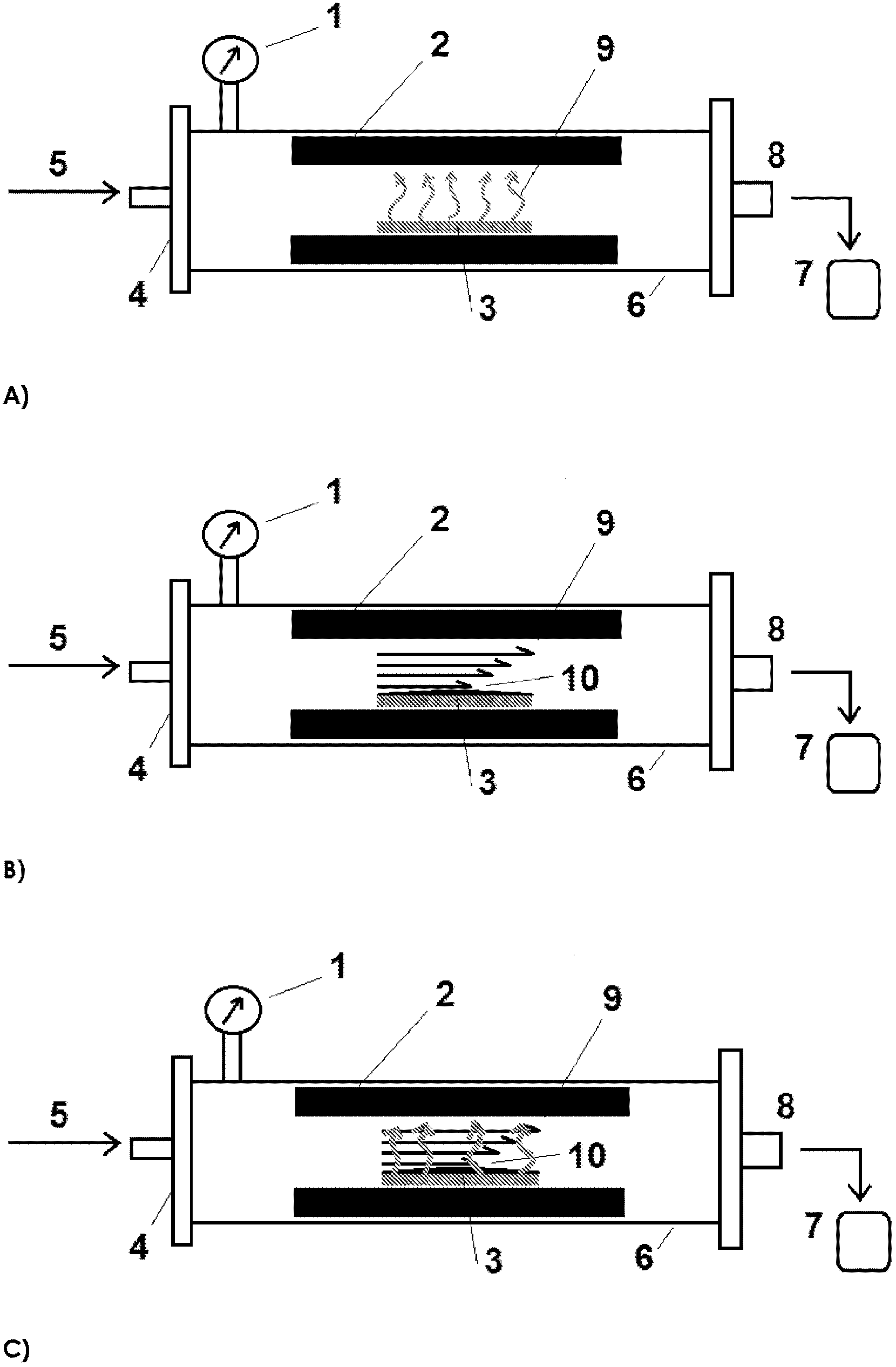
[0041] The method is similar to that described in Example 1, the only difference being that sublimation takes place for a very short time: at a pressure of 100 mbar, an argon flow of 26 l / min in 10 seconds or a flow of 4 minutes Reduce to 20 l / min. In this way, the growth of small targets (islands) of carbon 11 is induced on the surface of the SiC substrate 3 by initiating sublimation within a suitably short time ( image 3 D). Carbon islands 11 can optionally be used for subsequent graphene growth as nuclei obtained by sublimation. Figure 5 A tunneling microscope image showing isolated graphene islands is shown.

Embodiment 3

[0043] The method is similar to that described in Example 1, except that after etching, a low flow of Argon 10 (6 L / min at a pressure of 100 mbar) is applied, not allowing the sublimation of silicon from the substrate surface. Due to the CVD process and the gas (i.e. 2 ml / min of propane 12 ( image 3 E)) is introduced in the reactor, has carried out graphene growth. While silicon sublimation is suppressed under such conditions, the propane 12 molecules diffuse through the slowly shifting layers or the retarded gas into the substrate 3 surface. Thus, a graphene layer of controlled thickness is deposited on the SiC surface, which does not undergo sublimation. Control is accomplished by adjusting the timing and flow of propane 12 through the reactor. Separation of propane 12 ends the deposition. Graphene growth was performed on a SiC substrate 3 having (0001) and (000-1) surfaces. The obtained graphene is characterized by similar parameters to graphene obtained by sublimation...


PUM


Abstract

The present invention relates to a method for manufacturing graphene by vapour phase epitaxy on a substrate comprising a surface of SiC, characterized in that the process of sublimation of silicon from the substrate is controlled by a flow of an inert gas or a gas other than an inert gas through the epitaxial reactor. The invention also relates to graphene obtained by this method.

Description

technical field [0001] The present invention relates to a production method of graphene. More specifically, the present invention relates to a method of obtaining graphene by vapor phase epitaxy and a method of controlling its growth and nucleation during this process. Background technique [0002] Graphene is a flat two-dimensional sheet of carbon atoms arranged in a honeycomb shape on a hexahedral lattice, and each unit cell has two atoms (K.S.Novoselov et al. Science 306, 666 (2004); A.K.Geim, K.S.Novoselov, Nat . Mat. 6 (2007) 183; Y.B. Zhang, Y.W. Tan, H.L. Stormer and P. Kim, Nature 438, 201 (2005)). The carbon atoms are sp2 hybridized. Each of them is connected to three other carbon atoms by σ-type bonds. The electronic structure of graphene is quite different from common three-dimensional materials. Its Fermi surface is characterized by six double cones. In natural (undoped) graphene, the Fermi level is located at the junction of these cones. Since the density ...

Claims


Application Information

Patent Timeline
IPC IPC(8): C01B31/04C30B25/02C30B29/02C30B25/18C30B29/64
CPCC01B31/0461B82Y40/00B82Y30/00C01B32/186C01B32/188C30B25/025C30B25/18C30B29/02
Inventor 沃齐米日·施特鲁平斯基
Owner INST TECH MATERIAL ELEKT
Why Eureka
Try Eureka