Projection exposure device and splicing method

An exposure device and projection technology, applied in the field of lithography, can solve the problems of high requirements for splicing images, displacement of one image point, distortion of projected images, etc., and achieve the effect of improving exposure quality

Active Publication Date: 2013-03-06
SHANGHAI MICRO ELECTRONICS EQUIP (GRP) CO LTD
View PDF5 Cites 8 Cited by
  • Summary
  • Abstract
  • Description
  • Claims
  • Application Information

AI Technical Summary

Problems solved by technology

In an ideal state, the exposure can be completed by pattern splicing, but the projected image will be distorted, which will cause an image point to be displaced from the ideal position. For example, for a line with a line width of 2 microns, the relative distortion is often less than 0.1 micron. To ensure better overlay accuracy, it is difficult for traditional projection lithography machines to solve

Method used


Image

  • Projection exposure device and splicing method
  • Projection exposure device and splicing method
  • Projection exposure device and splicing method

Examples


no. 1 approach

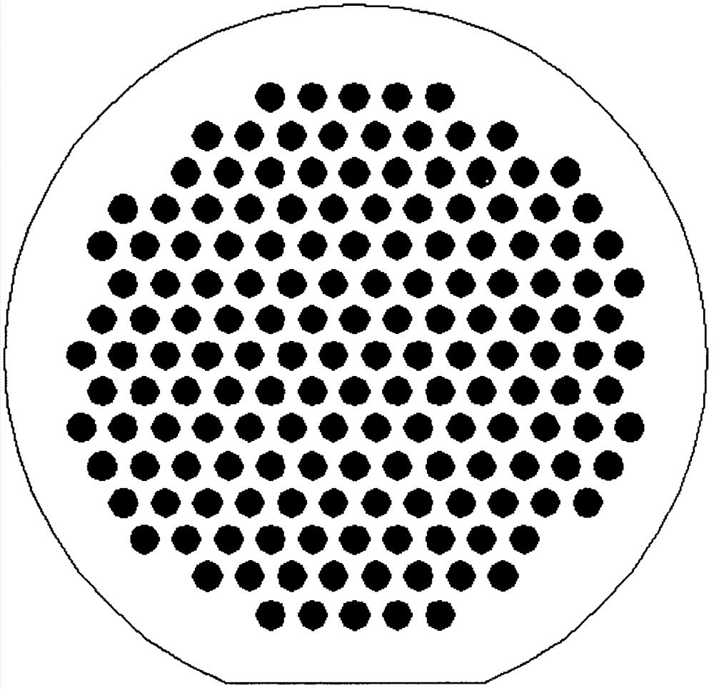
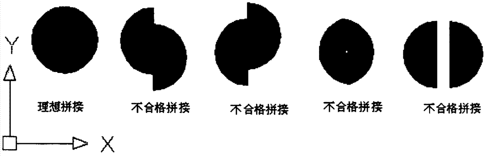
[0049] In this embodiment, the sapphire material with a diameter of 50 mm is used as the substrate, and the exposed circular patterns need to be arranged in a diamond shape. The diameter of the pattern is 2 microns, and the pattern spacing is 1 micron. The schematic diagram of the arrangement is as follows Figure 9 shown. The initial state of the four blades is as follows Figure 6 shown. Rotate the knife edges 9 and 11 clockwise by 30 degrees each, so that the stitching line between the fields of view does not pass through the graphics area, and the diamond-shaped field of view is as follows Figure 9 As shown, all four sides of the field of view are 0.5 μm from the edge of the graph. The action steps to form the diamond-shaped field of view are:

[0050] 1. First, the 9 blades are rotated 30 degrees clockwise with the upper left corner as the origin;

[0051] 2. Then the 11 knife edge is rotated 30 degrees clockwise with the upper right corner as the origin;

[0052] 3...

no. 2 approach

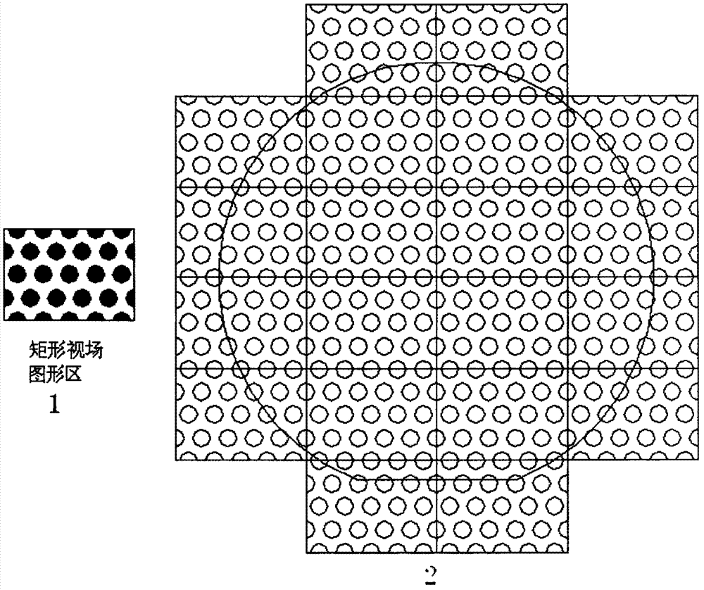
[0066] Figure 16 Shown is the exposure schematic diagram of the stepper photolithography machine adopting two kinds of fields of view: equilateral triangle field of view and trapezoidal field of view according to the present invention. The formation methods of equilateral triangular field of view and trapezoidal field of view are similar to the formation of prismatic field of view in Example 1. The use of these two non-rectangular fields of view can also avoid the pattern being divided by splicing lines, and its movement mode is similar to that of traditional stepping Lithography machines are the same. As shown in 20 , the triangular field of view first exposes area 1 on the substrate field by field, and then rotates the substrate 180 degrees horizontally, and then exposes area 2 on the substrate field by field. The trapezoidal field of view used in 21 is similar to the equilateral triangle field of view. First, the area 1 on the substrate is exposed field by field, and then...

no. 3 approach

[0075] The third method of the present invention is to adopt traditional methods such as Figure 6 For the rectangular field of view shown, the mask shape is made as Figure 9 or Figure 12 the rhombus shown or Figure 14 For non-rectangular shapes such as triangles shown, when the mask shape is made into a rhombus, the movement of the workbench of the lithography machine is as follows figure 2 Shown is similar to Example 1. Its workflow is:

[0076] 1. Put the mask into the mask holder through the transmission system;

[0077] 2. Transfer the 4-inch sapphire substrate to the top of the workpiece table, put it down, start the vacuum adsorption, and adsorb the substrate on the vacuum suction cup;

[0078] 3. According to the shape of the field of view, such as Figure 12 In the step-by-step recipe shown, the workpiece table is moved to move the desired exposure area of ​​the substrate to the bottom of the mask and expose each field of view one by one.

[0079] Figure ...


PUM

PropertyMeasurementUnit
Diameteraaaaaaaaaa

Abstract

A projection exposure device used for forming an exposure pattern on the surface of a substrate comprises a variable slit comprising a plurality of edges, the edges of the variable slit can translationally move and also can rotatably move, and the edges are adjusted according to the arrangement of the pattern to be exposed to adjust the shape and the dimension of the view field of the variable slit in order to make the view field margin traverse through the pattern to be exposed or in order to make the view field comprise the area of the pattern to be exposed, so a splicing line between the view field does not traverse the exposure pattern.

Description

technical field [0001] The invention relates to the field of photolithography, in particular to a projection exposure device in a photolithography device, and a projection exposure and splicing method. Background technique [0002] In the processing technology of high-brightness light-emitting diode HBLED, GaN-based LED epitaxy is prepared on a sapphire substrate. Since the lattice constants of GaN and sapphire substrate materials differ by 14%, the carrier generation rate is reduced, a large amount of heat energy is generated, and the life of the chip is shortened. The patterned sapphire substrate PSS technology can effectively improve the internal quantum efficiency of the chip, change the LED optical route, and improve the external quantum effect of the LED. [0003] The process flow of PSS is to first produce periodic patterns on the sapphire substrate by photolithography, such as figure 1 As shown, a circular pattern is photoetched on a 2-inch or 4-inch circular subst...

Claims


Application Information

Patent Timeline
IPC IPC(8): G03F7/20
Inventor 张俊唐世弋陈勇辉
Owner SHANGHAI MICRO ELECTRONICS EQUIP (GRP) CO LTD
Why Eureka
Try Eureka