SOI-LIGBT (Silicon on Insulator-Lateral Insulated-Gate Bipolar Transistor) device based on double channel structure

A dual-channel, device technology, applied in semiconductor devices, electrical components, circuits, etc., can solve the problems of device burnout failure, loss of gate control ability, etc., to achieve complete manufacturing process compatibility, good reliability, and strong anti-latch-up ability Effect

Inactive Publication Date: 2013-03-06
ZHEJIANG UNIV
View PDF3 Cites 5 Cited by
  • Summary
  • Abstract
  • Description
  • Claims
  • Application Information

AI Technical Summary

Problems solved by technology

When working with high current, when both transistors T1 and T2 are turned on and positive feedback is formed, a latch-up effect occurs inside the SOI-LIGBT device, causing it to lose its gate control capability, and it is in a high current working state for a long time, eventually causing the device to burn out and fail

Method used


Image

  • SOI-LIGBT (Silicon on Insulator-Lateral Insulated-Gate Bipolar Transistor) device based on double channel structure
  • SOI-LIGBT (Silicon on Insulator-Lateral Insulated-Gate Bipolar Transistor) device based on double channel structure
  • SOI-LIGBT (Silicon on Insulator-Lateral Insulated-Gate Bipolar Transistor) device based on double channel structure

Examples


Embodiment Construction

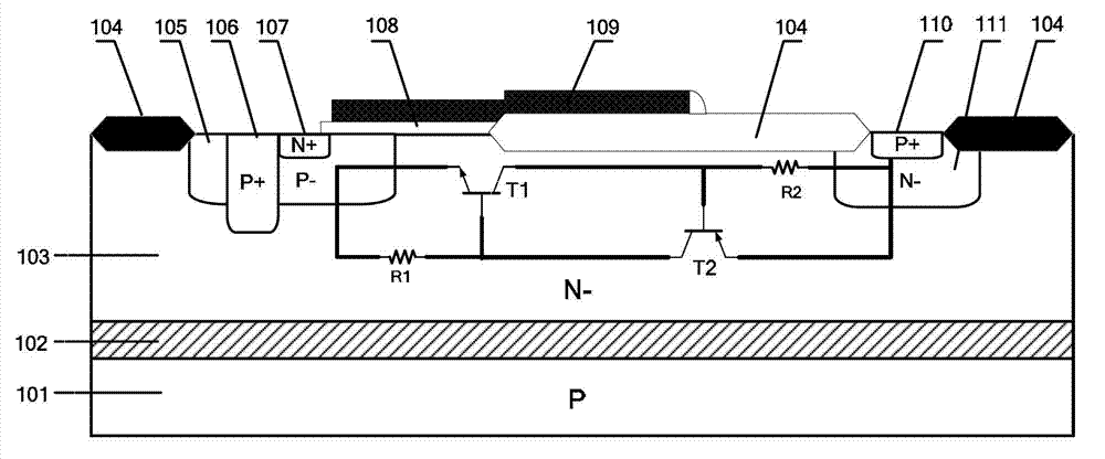
[0032] In order to describe the present invention more specifically, the technical solutions and related principles of the present invention will be described in detail below in conjunction with the accompanying drawings and specific embodiments.

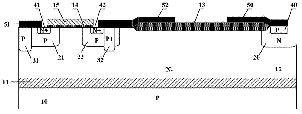
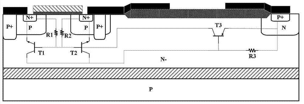
[0033] Such as figure 2 As shown, an SOI-LIGBT device based on a double-channel structure includes: a P-type substrate 10;

[0034] A buried oxide layer 11 is laid on the P-type substrate 10, an N- epitaxial layer 12 is laid on the buried oxide layer 11, an N well 20 is arranged on the N- epitaxial layer 12, and a P+ collector region 40 is embedded on the N well 20 , the P+ collector region 40 is provided with a metal electrode 50; on the N- epitaxial layer on one side of the P+ collector region 40, two mutually symmetrical body region structures are arranged side by side; wherein the second body region structure and the P+ collector region 40 adjacent;

[0035] The first body region structure includes a P well 21 arranged on the...


PUM


Abstract

The invention discloses an SOI-LIGBT (Silicon on Insulator-Lateral Insulated-Gate Bipolar Transistor) device based on a double channel structure. The SOI-LIGBT apparatus based on the double channel structure comprises a P type substrate, wherein a buried oxide layer is paved on the P type substrate, an N-epitaxial layer is paved on the buried oxide layer, a P+ collector region is embedded on the N-epitaxial layer, and two symmetrical body region structures are arranged in parallel on the N-epitaxial layer on one side of the P+ collector region. Each body region structure comprises a P well arranged on the N-epitaxial layer, an N+ emitter region embedded on the P well and a P+ contact region penetrating through the P well. According to the SOI-LIGBT device based on the double channel structure provided by the invention, two channel regions are arranged at the emitter region so that the cavity current flowing from the collector to the emitter is uniformly divided into two strands of current, therefore, the current flowing through a base electrode of a parasitic NPN triode is reduced to 50% of the total current. A parasitic thyristor is inhibited from being opened and the anti-latch capacity of the device is improved, so that the reliability of the device is improved.

Description

technical field [0001] The invention belongs to the technical field of semiconductor devices, in particular to an SOI-LIGBT device based on a double-channel structure. Background technique [0002] LIGBT (Lateral Insulated-Gate Bipolar Transistor, Lateral Insulated Gate Bipolar Transistor) is a combination of the advantages of power MOSFET (easy to drive, simple control, fast switching speed) and the advantages of bipolar transistors (large current handling capacity, saturation voltage Reduced, low switching loss) transistors are an indispensable power "core" in the electronics industry, and are widely used in the output stage of power output drive circuits. The SOI (Silicon On Insulator, silicon on insulator) technology is widely used in the manufacture of power integrated circuits due to its ideal dielectric isolation performance. The SOI-LIGBT device is a LIGBT device manufactured based on SOI technology. Since it is completely isolated from the substrate and other high-...

Claims


Application Information

Patent Timeline
Patent Type & Authority Applications(China)
IPC IPC(8): H01L29/10H01L29/739
Inventor 张世峰韩雁张斌张炜吴焕挺
Owner ZHEJIANG UNIV
Why Eureka
Try Eureka