Seed crystal for aluminium nitride (ALN) crystal growth

A technology of crystal growth and seed crystal, applied in crystal growth, single crystal growth, single crystal growth and other directions, can solve the problems of high impurity content of AlN crystals, difficult to obtain large-sized AlN crystals, etc. simple craftsmanship

Active Publication Date: 2013-03-27
HARBIN INST OF TECH
View PDF3 Cites 12 Cited by
  • Summary
  • Abstract
  • Description
  • Claims
  • Application Information

AI Technical Summary

Problems solved by technology

[0008] The purpose of the present invention is to solve the existing problem that it is difficult to obtain large-sized AlN crystals by spontaneous nucleation, and the AlN crystals grown by the heterogeneous seed crystal method have high impurity content, and provide a seed crystal for AlN crystal growth

Method used


Image

  • Seed crystal for aluminium nitride (ALN) crystal growth
  • Seed crystal for aluminium nitride (ALN) crystal growth

Examples


specific Embodiment approach 1

[0038] Specific Embodiment 1: The seed crystal used for AlN crystal growth in this embodiment is an AlN ceramic sheet after annealing process. The diameter of the AlN ceramic sheet is 1~4 inches, the thickness is 0.3~5mm, and the surface roughness Ra≤15nm .

specific Embodiment approach 2

[0039] Specific embodiment two: the difference between this embodiment and specific embodiment one is that the annealing process is implemented through the following steps:

[0040] 1. After heating and corroding the AlN ceramic sheet in strong acid or strong alkali, clean the surface of the AlN ceramic sheet with alcohol or acetone, and then dry it with nitrogen to obtain the cleaned AlN ceramic sheet;

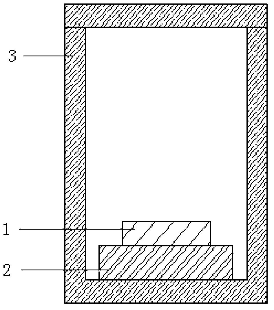
[0041] 2. Put the cleaned AlN ceramic sheet obtained in step 1 on the TaC sheet and put it into the TaC crucible, put the TaC crucible into the high-temperature annealing equipment, and evacuate to 5×10 -4 ~6×10 -4 Pa, into 0.6~1atm nitrogen or argon, then heated to 400~600°C at a heating rate of 10~15°C / min, and then heated to 1800 at a heating rate of 5~10°C / min after holding for 0.5~1 hour ~2100°C, keep warm for 3~8 hours, and then cool down to room temperature at a rate of less than 5°C / min to obtain seed crystals for AlN crystal growth;

[0042] Wherein the step one de...

specific Embodiment approach 3

[0045] Specific Embodiment Three: The seed crystal used for AlN crystal growth in this embodiment is an AlN ceramic sheet that has been annealed and then polished. The diameter of the AlN ceramic sheet is 1 to 4 inches, the thickness is 0.3 to 5 mm, and the surface is rough. Degree Ra≤6nm.

[0046] In this embodiment, the AlN ceramic sheet after the high-temperature annealing process is polished, and the AlN ceramic seed crystal after polishing is nucleated on the surface of the AlN crystal, and the grain size is more uniform, there is no abnormally grown grain, and more It is beneficial to improve the growth quality of AlN crystal.


PUM

PropertyMeasurementUnit
diameteraaaaaaaaaa
thicknessaaaaaaaaaa
surface roughnessaaaaaaaaaa

Abstract

A seed crystal for aluminium nitride (ALN) crystal growth relates to a material for ALN crystal growth. A problem that spontaneous nucleation adopted at current is difficult to obtain a big-size ALN crystal and an impurity content of the ALN crystal grown by an alloplasm seed crystal method is high is solved. The seed crystal for ALN crystal growth is an ALN ceramic wafer after treatment of annealing process. The seed crystal for ALN crystal growth further can be an ALN ceramic wafer after treatment of annealing process and polishing in sequence, or an ALN thin film is pasted on the surface of a polished seed crystal to obtain the seed crystal for ALN crystal growth. The ALN crystal grown by using the seed crystal for ALN crystal growth is big in size and fewer in impurity content. The seed crystal is mainly applied to growth of the ALN crystal in a semiconductor device.

Description

technical field [0001] The invention relates to a material for AlN crystal growth. Background technique [0002] AlN crystal is an important wide bandgap (6.2eV) semiconductor material with high thermal conductivity (3.2W cm -1 ·K -1 ), high resistivity (10 13 ~10 15 Ω·m) and high surface acoustic velocity (5600~6000m / s) and other excellent physical properties, are widely used in semiconductor devices such as lasers, high-power electronic devices, optoelectronic devices and surface acoustic wave devices. [0003] At present, the physical vapor transport (Physical Vapor Transport, PVT) method is recognized as one of the effective ways to prepare large-sized AlN crystals. In the process of spontaneous nucleation and growth of AlN crystals by PVT method, the nucleation stage in the early stage of crystal growth is the most important growth stage, but this stage is difficult to control, which is manifested in the uniformity of spontaneous nucleation, nucleation size and nucl...

Claims


Application Information

Patent Timeline
Patent Type & Authority Applications(China)
IPC IPC(8): C30B29/38C30B23/00
Inventor 韩杰才宋波金雷张化宇
Owner HARBIN INST OF TECH
Why Eureka
Try Eureka