Multilayer printed circuit board and manufacturing method thereof

A multi-layer printing and circuit board technology, applied in the direction of multi-layer circuit manufacturing, printed circuit components, circuit substrate materials, etc., can solve the problems of high cost of printed circuit boards, easy water absorption of FR-4, and poor resistance to voltage, etc. Achieve the effect of less difficulty in processing, good insulation and mechanical strength, and low cost

Inactive Publication Date: 2013-03-27
SHENZHEN WUZHU TECH
View PDF6 Cites 1 Cited by
  • Summary
  • Abstract
  • Description
  • Claims
  • Application Information

AI Technical Summary

Problems solved by technology

[0003] In the prior art, epoxy resin as the main body (FR-4) is currently the largest and most widely used type of product for printed circuit boards. However, printed circuit boards made of FR-4 materials have high cost and large dielectric loss. And the electrical performance is poor, and FR-4 has a series of shortcomings such as easy water absorption, easy aging, and poor voltage resistance, which makes the printed circuit boards made of it not suitable for special environments, especially humid environments, aerospace, high-speed, etc. Communications, space or radioactive medical devices) and other fields require materials with light density, low transmission dielectric loss, strong corrosion resistance, environmental protection, and high insulation.

Method used


Image

  • Multilayer printed circuit board and manufacturing method thereof
  • Multilayer printed circuit board and manufacturing method thereof
  • Multilayer printed circuit board and manufacturing method thereof

Examples


Embodiment Construction

[0033] Specific embodiments of the present invention will be described in detail below in conjunction with the accompanying drawings.

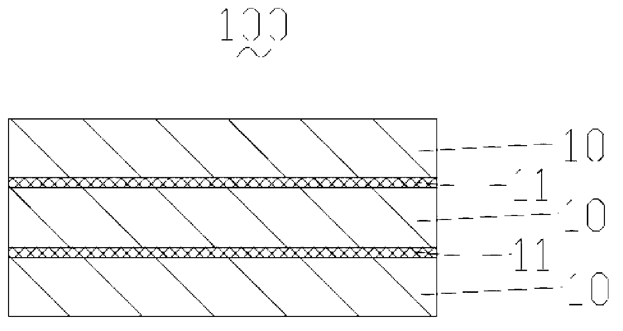
[0034] see figure 1 , figure 1 It is a schematic cross-sectional structure diagram of a multilayer printed circuit board (Printed Circuit Board, PCB) of the present invention. The multi-layer printed circuit board 100 has at least a plurality of single-layer printed circuit boards 10 and a plurality of adhesive layers 11 for bonding the plurality of single-layer printed circuit boards 10 . For the convenience of describing the present invention, figure 1 The illustrated multilayer printed circuit board 100 comprises three single layer printed circuit boards 10 and two adhesive layers 11 .

[0035] Specifically, the plurality of single-layer printed circuit boards 10 and the plurality of adhesive layers 11 are layered structures, which are alternately stacked, that is, a single-layer printed circuit board 10 plus an adhesive layer The lamin...


PUM


Abstract

The invention relates to a manufacturing method for a multilayer printed circuit board. The method comprises steps of providing at least two single-layer printed circuit boards which respectively comprise a substrate and a copper layer arranged on the surface of the substrate which is made of polymethyl methacrylate materials; providing at least one bonding layer and enabling the single-layer printed circuit boards and the bonding layer to be stacked in stagger; and conducting thermocompression bonding on a stack structure of the single-layer printed circuit boards and the bonding layer, enabling the two single-layer printed circuit boards to be tightly bonded through the bonding layer and forming the multilayer printed circuit board. The invention further provides the multilayer printed circuit board manufactured by using the manufacturing method for the multilayer printed circuit board. The multilayer printed circuit board and the manufacturing method have the advantages of being excellent in electric and mechanical performance, wide in applicable scope, low in cost and simple in manufacture method.

Description

technical field [0001] The invention relates to a multilayer printed circuit board and its manufacturing method, in particular to a multilayer printed circuit board with PMMA (polymethyl methacrylate) as the substrate and thermoplastic polyurethane elastomer as the adhesive layer and its manufacturing method . Background technique [0002] Printed Circuit Board (PCB) is the basis of almost any electronic product. With the rapid development of the electronics industry, printed circuit boards, as the basic components of electronic products, are more and more widely used. Although the functions of electronic products are not only enhanced, the application With the expansion of the field, especially driven by the development of the high-speed information age, there are more and more requirements for printed circuit boards used in electronic products, especially the requirements for printed circuit boards in terms of signal transmission quality and speed. constantly improving. ...

Claims


Application Information

Patent Timeline
Patent Type & Authority Applications(China)
IPC IPC(8): H05K1/03H05K3/46
Inventor 曾志徐学军田国任威
Owner SHENZHEN WUZHU TECH
Why Eureka
Try Eureka