Silicon carbide substrate, semiconductor device, and SOI wafer
A technology of silicon carbide substrate and silicon carbide, which is applied in the direction of semiconductor devices, semiconductor/solid-state device manufacturing, semiconductor/solid-state device components, etc., can solve the problem of substrate materials that are not suitable for carrying high-frequency semiconductor components, large loss of silicon carbide, etc. problem, to achieve excellent heat dissipation, low frequency loss effect
- Summary
- Abstract
- Description
- Claims
- Application Information
AI Technical Summary
Problems solved by technology
Method used
Image
Examples
Embodiment 1
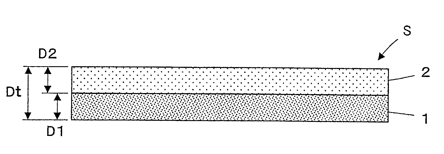
[0036] figure 1 The silicon carbide substrate S of Example 1 is shown. The silicon carbide substrate S has a two-layer structure including a first silicon carbide layer 1 having a thickness D1 and a second silicon carbide layer 2 having a thickness D2 formed on the surface of the first silicon carbide layer 1 . The first silicon carbide layer 1 and the second silicon carbide layer 2 are both composed of polycrystalline silicon carbide, the second silicon carbide layer 2 has a smaller high-frequency loss than the first silicon carbide layer 1, and the first silicon carbide layer 1 It has higher thermal conductivity than the second silicon carbide layer 2 in the thickness direction.
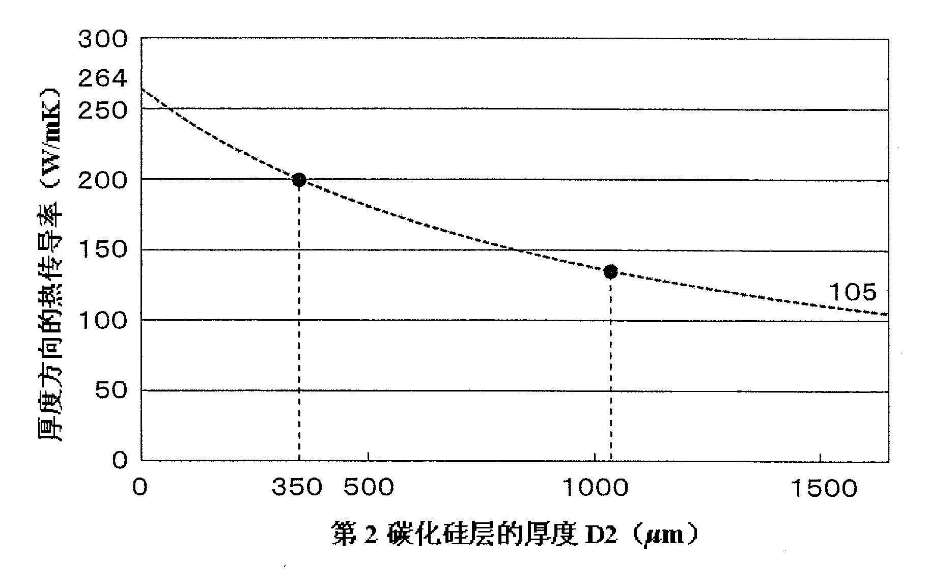
[0037] For example, the thermal conductivity of the second silicon carbide layer 2 is about 100 W / mK relative to the thermal conductivity of the first silicon carbide layer 1 of 260 W / mK.
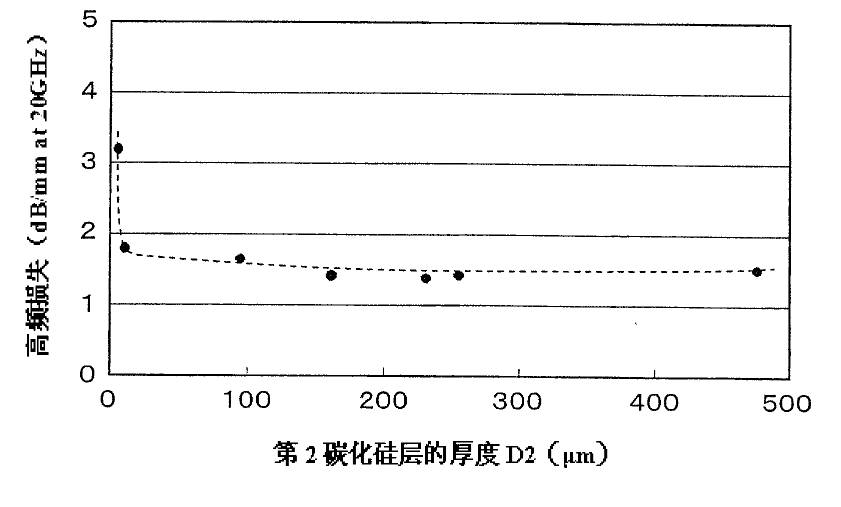
[0038] In addition, the high-frequency loss at a frequency of 20 GHz has a large value of about 50 dB / mm wi...
Embodiment 2
[0060] Figure 4 The structure of the semiconductor device of Example 2 is shown. In this semiconductor device, a semiconductor element 3 is bonded to the surface of the second silicon carbide layer 2 of the silicon carbide substrate S shown in the first embodiment. Semiconductor element 3 is bonded to the surface of second silicon carbide layer 2 by brazing or the like. Alternatively, a specific conductive pattern may be formed on the surface of the second silicon carbide layer 2, and the semiconductor element 3 may be bonded to the conductive pattern by solder.
[0061] According to the semiconductor device with such a structure, the silicon carbide substrate S has a small high-frequency loss of 2 dB / mm or less at a frequency of 20 GHz on the surface side of the second silicon carbide layer 2 on the mounting surface of the semiconductor element 3, and 200 W / mK or more. High thermal conductivity, even if the semiconductor element 3 is an element operating in a high-frequenc...
Embodiment 3
[0064] Figure 5 The structure of the SOI (Silicon on Insulator) wafer of Example 3 is shown. The SOI wafer is formed with SiO on the surface of the second silicon carbide layer 2 of the silicon carbide substrate S shown in Example 1. 2 Simultaneously with the insulating layer 4 , a silicon layer 5 is formed on the surface of the insulating layer 4 . Circuit elements are formed using the silicon layer 5 .
[0065] In this SOI wafer, the silicon carbide substrate S also has a small high-frequency loss of 2 dB / mm or less at a frequency of 20 GHz on the surface side of the second silicon carbide layer 2, and a thermal conductivity of 200 W / mK or more. Layer 5 is used to form an element operating in a high-frequency region, and a highly reliable device capable of rapid operation can also be realized.
[0066] In addition, the silicon carbide substrate S has 10 on the surface side of the second silicon carbide layer 2 4 A high specific resistance of Ωcm or more enables highly r...
PUM
| Property | Measurement | Unit |
|---|---|---|
| thickness | aaaaa | aaaaa |
Abstract
Description
Claims
Application Information


