Etching method of semiconductor structure

A semi-conductor technology to be etched, which is applied in semiconductor/solid-state device manufacturing, discharge tubes, electrical components, etc. It can solve the problem of slow etching rate and achieve uniform distribution

Active Publication Date: 2013-04-03
ADVANCED MICRO FAB EQUIP INC CHINA
View PDF5 Cites 9 Cited by
  • Summary
  • Abstract
  • Description
  • Claims
  • Application Information

AI Technical Summary

Problems solved by technology

However, the etching rate of the capacitively coupled plasma etching device of the prior art is relatively slow

Method used


Image

  • Etching method of semiconductor structure
  • Etching method of semiconductor structure
  • Etching method of semiconductor structure

Examples


Embodiment Construction

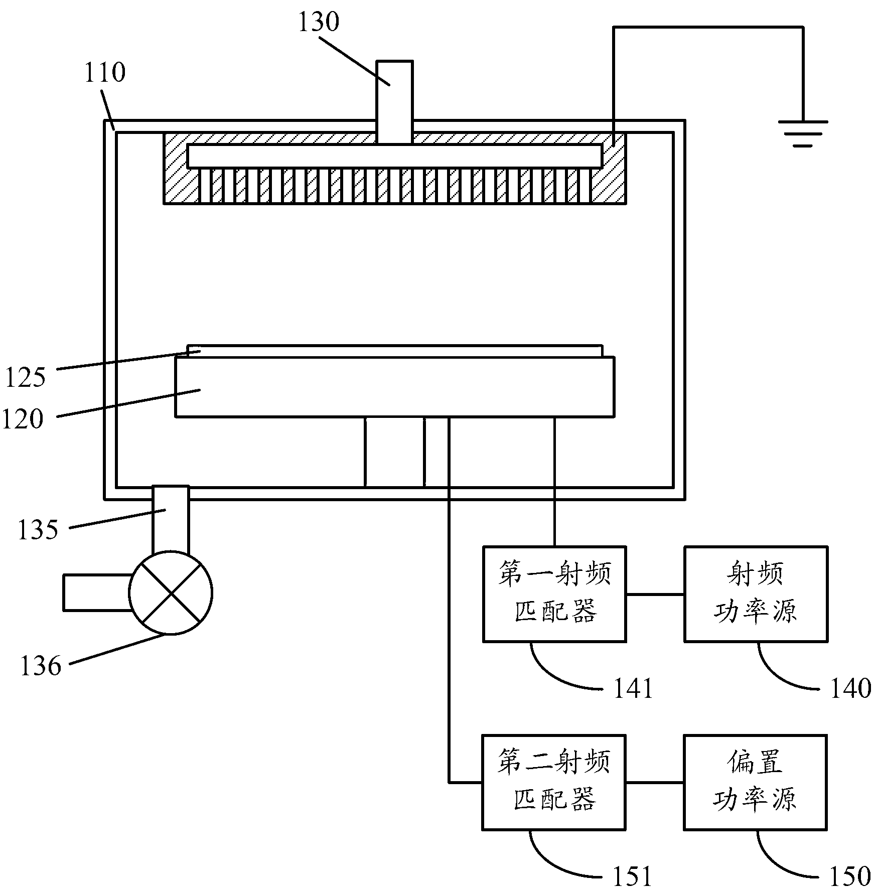
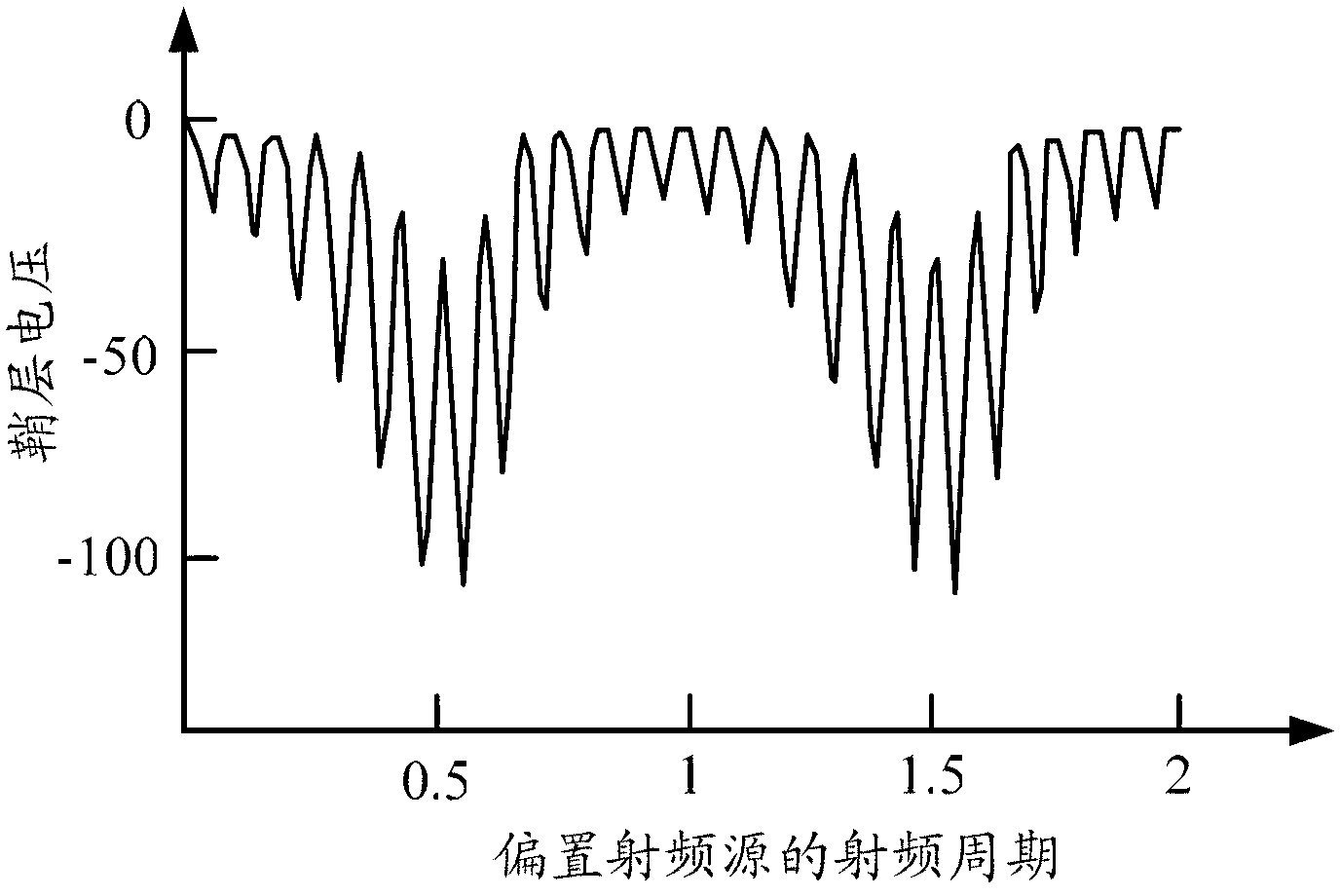
[0028] Since the positive ions and electrons in the plasma have different angular distributions, the positively charged positive ions tend to gather at the bottom of the etching opening formed by etching the material layer to be etched, and the continuous bias will make the etching The positively charged ions at the bottom of the etched opening are continuously gathered, and the micro-electric field formed by the positively charged ions will affect the trajectory of the subsequently arriving positively charged ions, so that the sidewall of the etched opening is over-etched, and the The etch rate at the bottom of the etched opening is slower, affecting the overall etch rate.

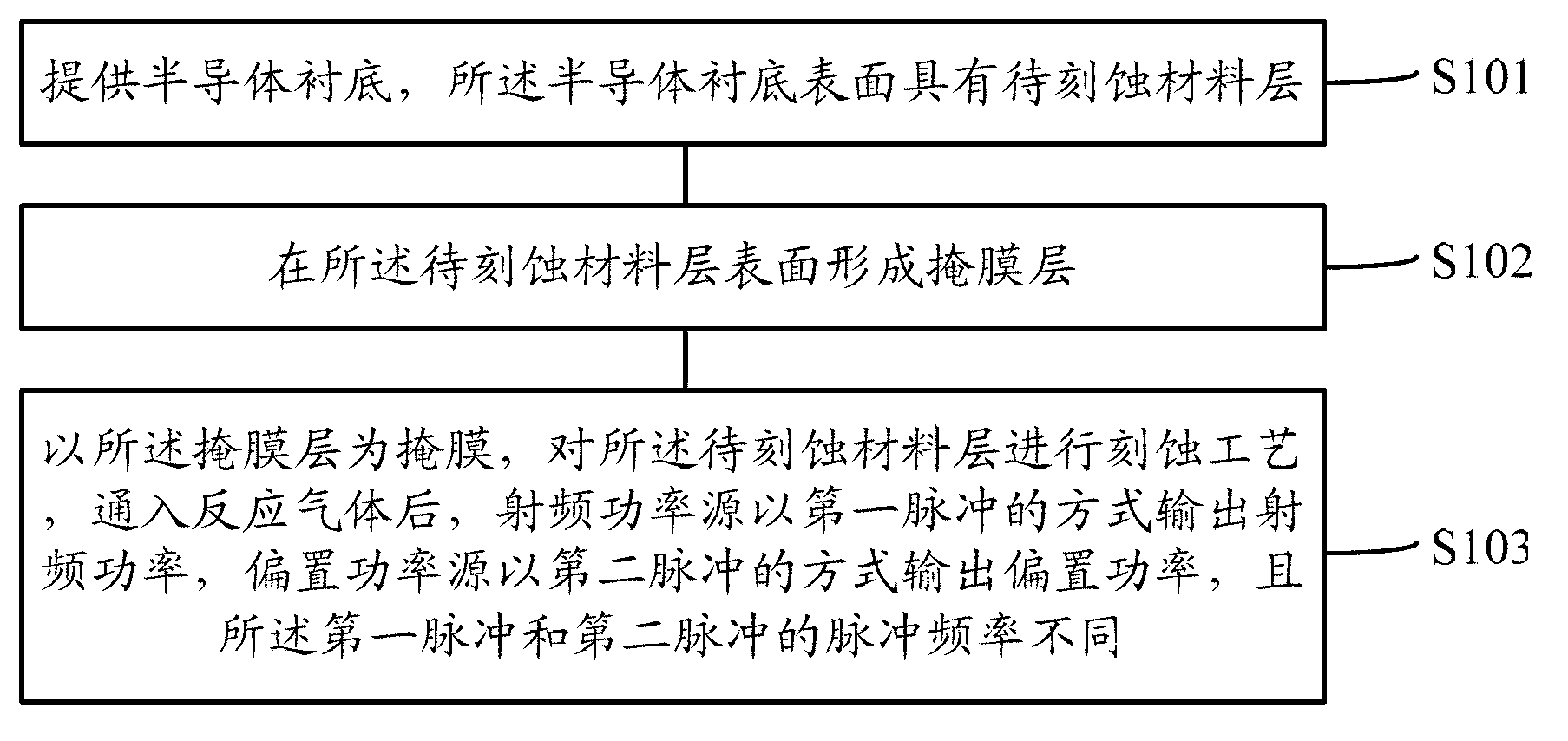
[0029] To this end, an embodiment of the present invention provides a method for etching a semiconductor structure. After the reactive gas is introduced, the RF power source outputs RF power in the form of a first pulse, and the bias power source outputs RF power in the form of a second pulse. The bias po...


PUM


Abstract

An etching method of a semiconductor structure includes: providing a semiconductor substrate with a to-be-etched material layer on the surface; forming a mask layer on the surface of the to-be-etched material layer; using the mask layer as a mask to etch the to-be-etched material layer, and allowing a radio-frequency power source to output radio-frequency power in a first pulse manner and a bias power source to output bias power in a second pulse manner after introducing reactant gas, wherein first pulse and second pulse are different in pulse frequency. Etching is fast. In addition, the size of an etching process window and the time-varying distribution of the etching speed can be regulated by controlling pulse frequency ratio of the radio-frequency power source to the bias power source.

Description

technical field [0001] The invention relates to semiconductor technology, in particular to an etching method for a semiconductor structure. Background technique [0002] In the semiconductor process, the process of etching the semiconductor material generally includes a dry etching process or a wet etching process, wherein, since the dry etching process using plasma for etching can effectively control the size of the etching opening The size has become the most mainstream etching process at present. Existing processes usually use glow discharge, radio frequency signal, corona discharge, etc. to form plasma. Among them, when using radio frequency signals to form plasma, the density and energy of the formed plasma can be controlled by adjusting the processing gas composition, frequency of radio frequency power, coupling mode of radio frequency power, air pressure, temperature and other parameters, so as to optimize the plasma treatment effect . Therefore, in existing semico...

Claims


Application Information

Patent Timeline
Patent Type & Authority Applications(China)
IPC IPC(8): H01J37/32H01L21/311
Inventor 王兆祥梁洁倪图强
Owner ADVANCED MICRO FAB EQUIP INC CHINA
Why Eureka
Try Eureka