Silicon on insulator (SOI) transverse high voltage power device with ultralow specific on resistance

A technology of specific on-resistance and lateral high voltage, which is applied in the field of SOI lateral high-voltage power devices, can solve the problems of increasing specific on-resistance of devices, achieve the effects of reducing the layout, slowing down the self-heating effect, and being easy to integrate

Active Publication Date: 2013-04-03
UNIV OF ELECTRONICS SCI & TECH OF CHINA
View PDF6 Cites 13 Cited by
  • Summary
  • Abstract
  • Description
  • Claims
  • Application Information

AI Technical Summary

Problems solved by technology

[0003] The technical problem to be solved by the present invention is that the traditional SOI lateral high-voltage power device adopts a drift region with a lower doping concentration in order to obtain a high withstand voltage, resulting in an increase in the specific on-resistance of the device, and the use of a thick buried oxide layer brings significant Self-heating effect and other issues, based on the theory of enhanced bulk field ENBULF (Enhanced Bulk Field), a SOI lateral high-voltage power device with low ultra-low specific on-resistance is proposed

Method used


Image

  • Silicon on insulator (SOI) transverse high voltage power device with ultralow specific on resistance
  • Silicon on insulator (SOI) transverse high voltage power device with ultralow specific on resistance
  • Silicon on insulator (SOI) transverse high voltage power device with ultralow specific on resistance

Examples


Embodiment Construction

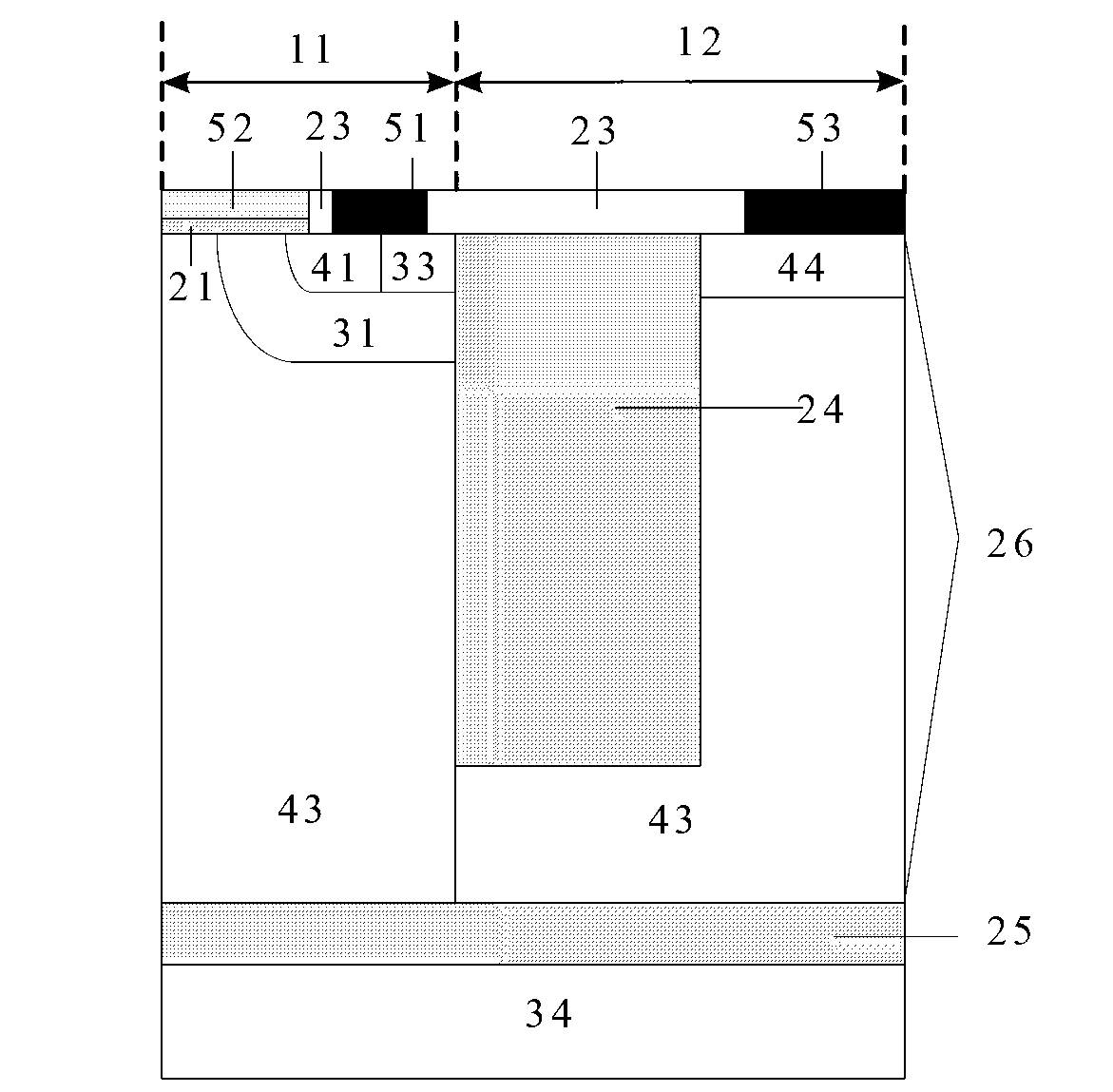
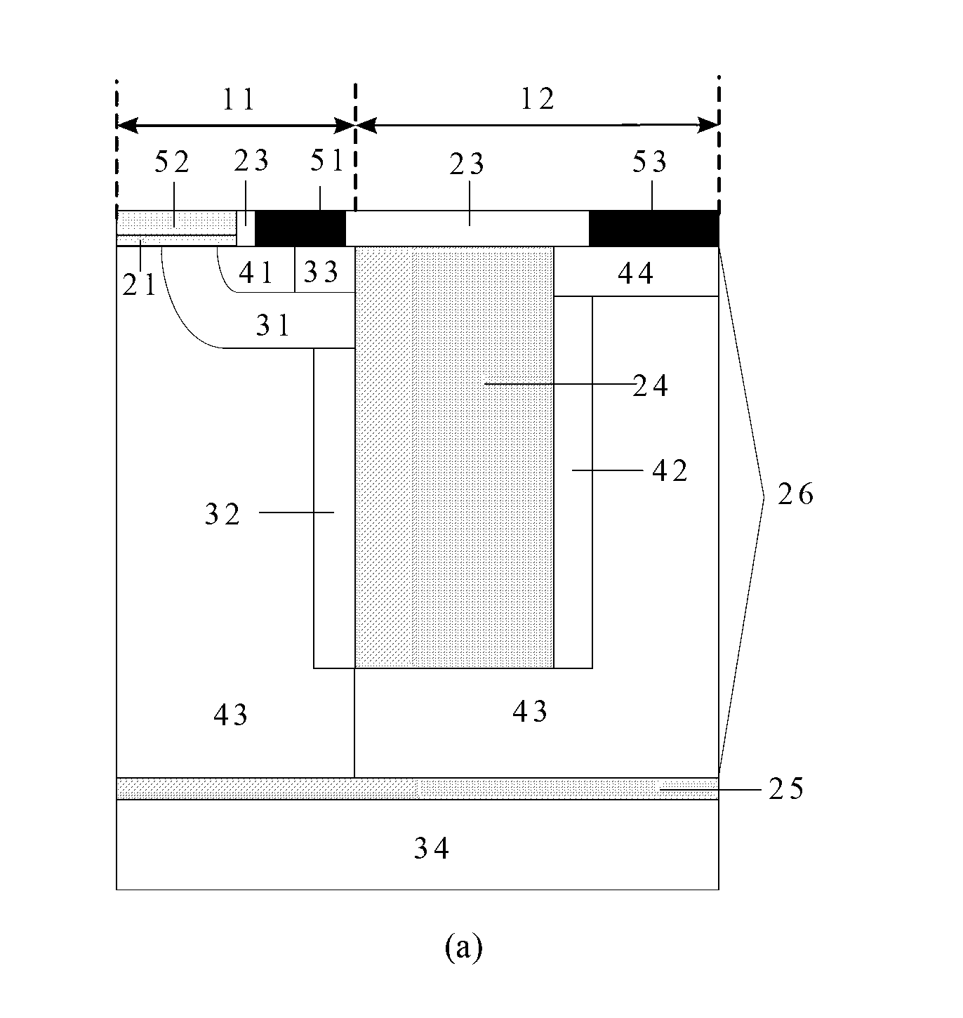
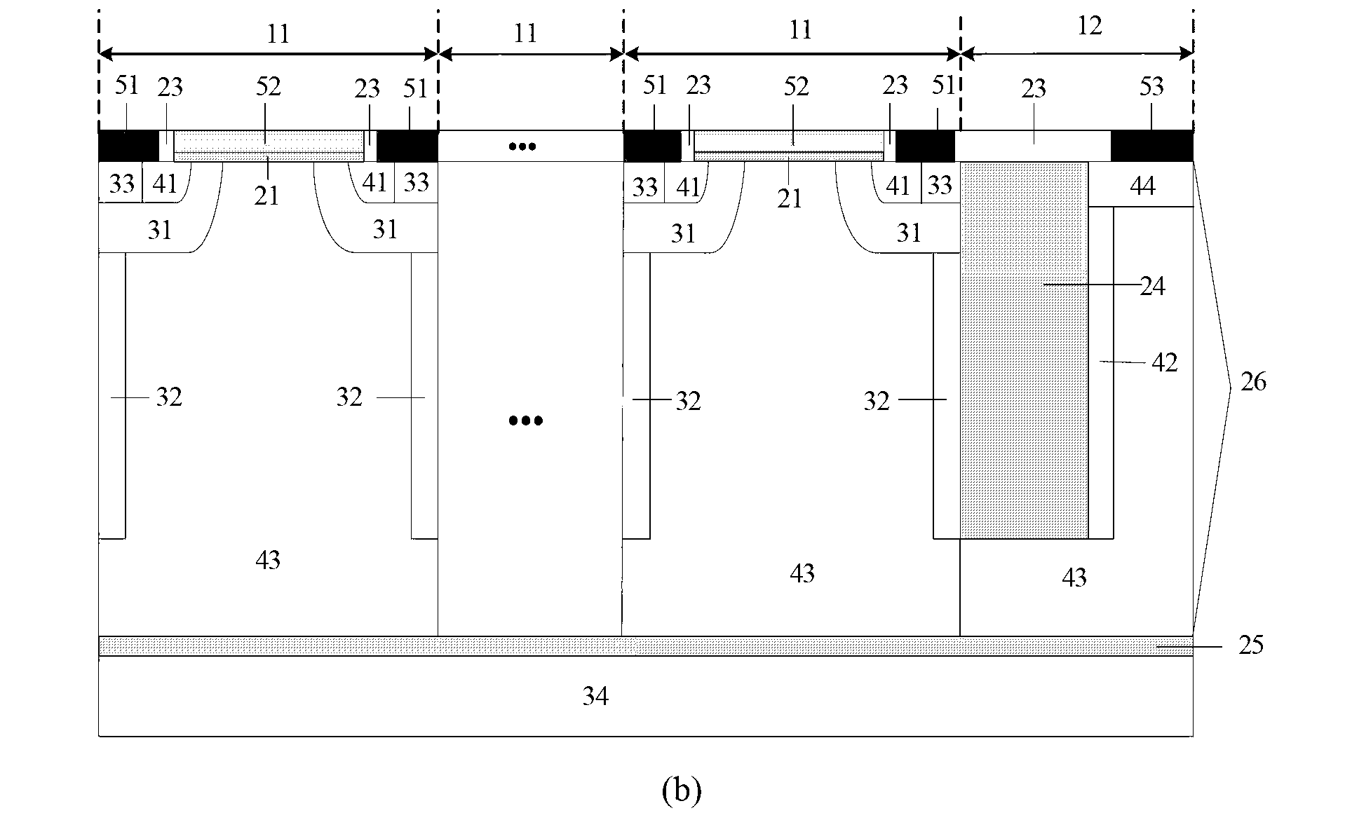
[0032] A SOI lateral high-voltage power device with ultra-low specific on-resistance, such as figure 2 As shown, at least one or more longitudinal superjunction cellular structures 11 and terminal structures 12 are included; multiple longitudinal superjunction cellular structures 11 are closely packed together along the lateral or width direction of the device to form an overall longitudinal superjunction cellular structure ; The terminal structure 12 is located on the outside or periphery of the overall cellular structure. The vertical superjunction cell structure 11 and the terminal structure 12 are made on the SOI layer 26 of the SOI material, and the SOI material includes a substrate layer 34, a buried oxide layer 25 and an SOI layer 26, wherein the buried oxide layer 25 is located on the substrate layer 34 and between the SOI layer 26 .

[0033] The vertical superjunction cell structure 11 includes an N-type drift region 43, a P-type well region 31 located outside the t...


PUM


Abstract

A silicon on insulator (SOI) transverse high voltage power device with ultralow specific on resistance belongs to the technical field of power semiconductor devices and comprises a vertical super junction cellular structure and a terminal structure. The terminal structure is located on the outside or the periphery of an integral cellular structure. The device is manufactured on an SOI layer of an SOI material. The vertical super junction cellular structure improves breakdown voltage, reduces specific on resistance simultaneously and reduces domain area. The device is integrated by a single cellular or a plurality of cellulars, the plurality of cellulars connected in parallel can share one terminal, and a drain leading out structure is utilized to lead out a drain transversely to enable the drain, a grid and a source to be located on the surface. The device can be easily integrated with a common circuit, greatly reduces domain area and further reduces process cost. In addition, the device is capable of increasing a device vertical electric field by adopting a thin oxygen burying layer and simultaneously can effectively relieve self-heating effect.

Description

technical field [0001] The invention belongs to the technical field of semiconductor power devices, and relates to an SOI lateral high-voltage power device with ultra-low specific on-resistance. Background technique [0002] Silicon On Insulator SOI (Silicon On Insulator) is a new type of material used in the manufacture of integrated circuits, which can replace bulk silicon that is currently widely used. The lateral high-voltage power device LDMOS (Lateral Double-diffused Metal Oxide Semiconductor) has extremely important uses in power integrated circuits and intelligent power circuits. The drain, source and gate of this type of device are all on the chip surface, which is easy to communicate with Low-voltage signal circuit integration simplifies the driving circuit of power devices. LDMOS made of SOI material has good isolation performance, small parasitic capacitance and leakage current, and the process is compatible with CMOS (Complementary Metal Oxide Semiconductor) pr...

Claims


Application Information

Patent Timeline
Patent Type & Authority Applications(China)
IPC IPC(8): H01L29/78H01L29/06
Inventor 乔明章文通许琬李燕妃张昕吴文杰张波
Owner UNIV OF ELECTRONICS SCI & TECH OF CHINA
Why Eureka
Try Eureka