Light-emitting diode grain and manufacturing method thereof

A technology of light-emitting diodes and manufacturing methods, which is applied to electrical components, circuits, semiconductor devices, etc., and can solve problems such as poor electrical properties and poor light transmission

Inactive Publication Date: 2013-04-03
ZHANJING TECH SHENZHEN +1
View PDF3 Cites 3 Cited by
  • Summary
  • Abstract
  • Description
  • Claims
  • Application Information

AI Technical Summary

Problems solved by technology

In the process of fabricating the transparent conductive layer structure on the semiconductor light-emitting structure of the light-emitting diode, when the transparent conductive layer is made thin, it has high light transmittance, but the electrical property is poor; when the transparent conductive layer is made thick, the electrical property is poor. Good performance but poor light transmission, so it is inevitable that there will be a trade-off between the light output and electrical properties of the light-emitting diode grains and cannot be balanced

Method used


Image

  • Light-emitting diode grain and manufacturing method thereof
  • Light-emitting diode grain and manufacturing method thereof

Examples


Embodiment Construction

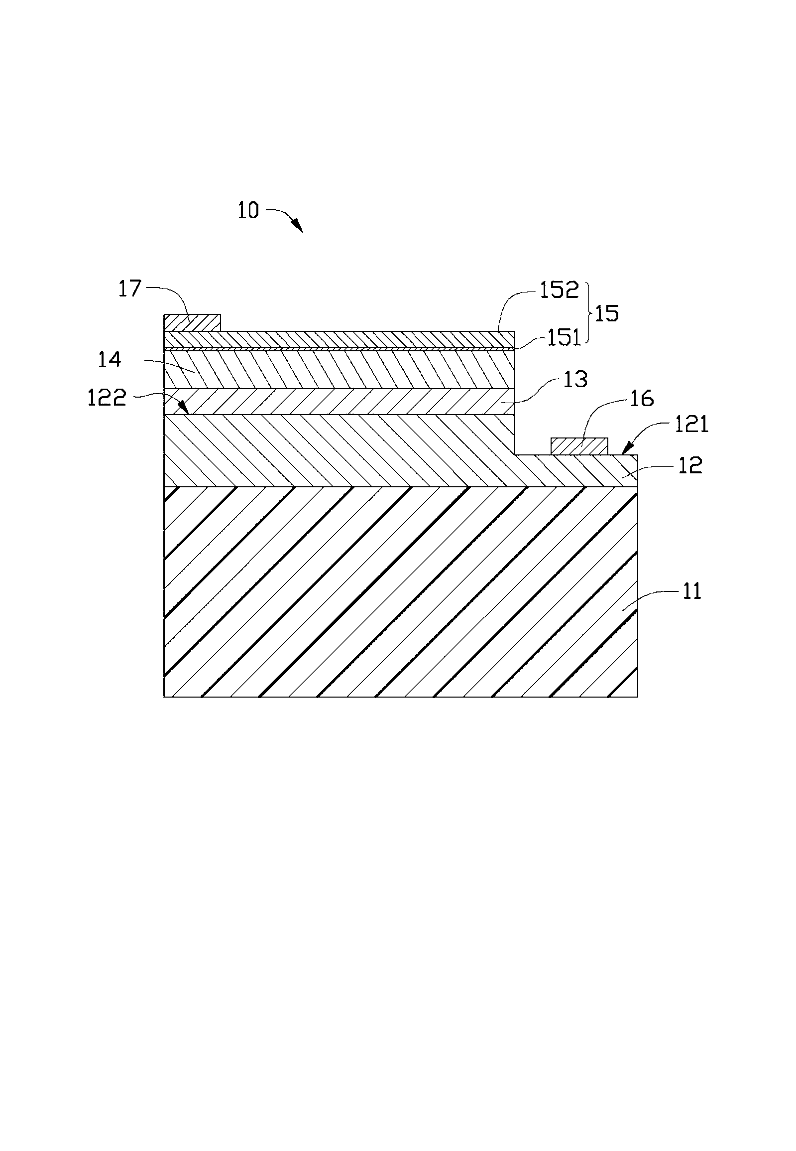
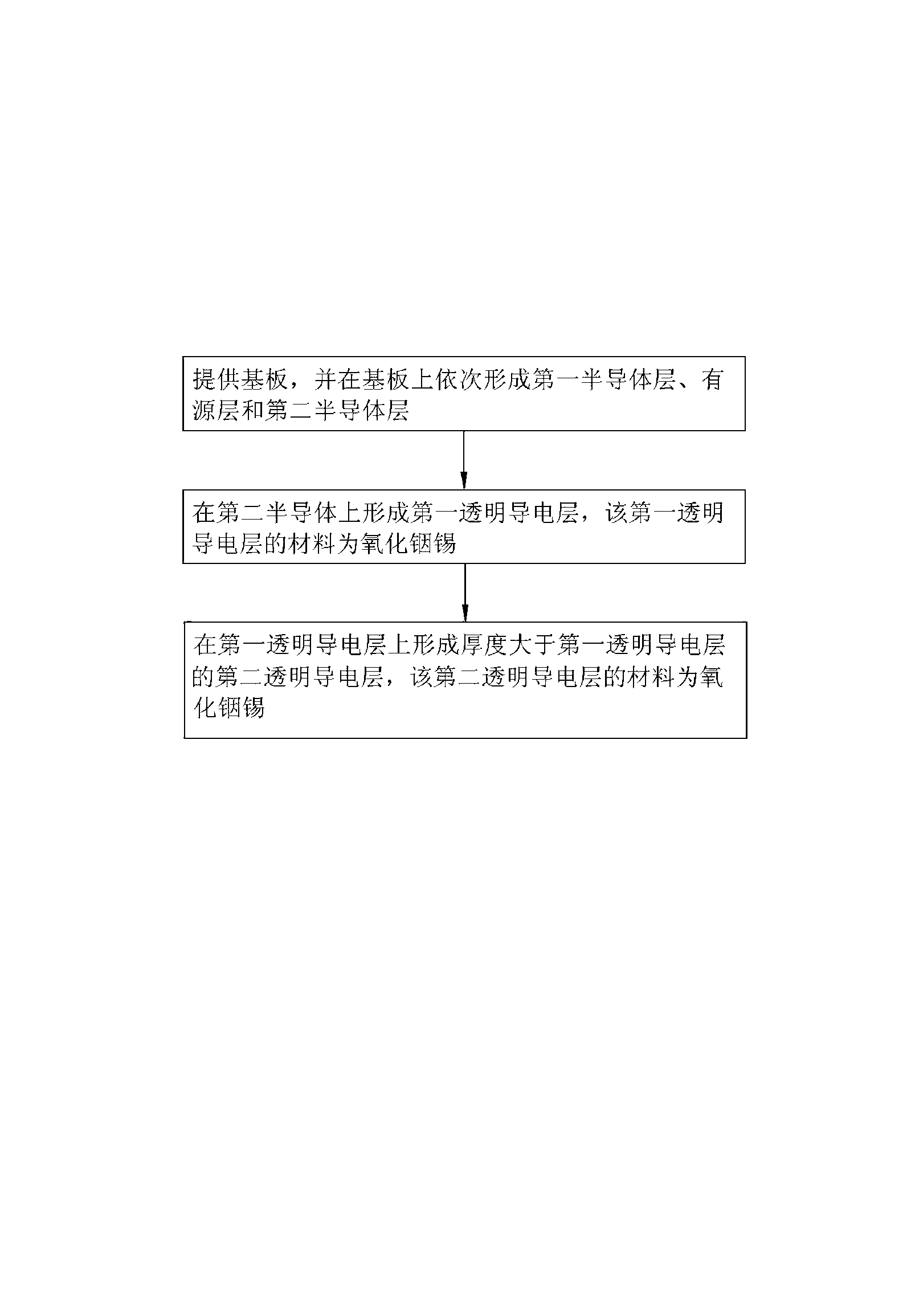
[0016] see figure 1 The light emitting diode die 10 provided by the embodiment of the present invention includes a substrate 11 , a first semiconductor layer 12 , an active layer 13 , a second semiconductor layer 14 , a transparent conductive layer 15 , a first electrode 16 and a second electrode 17 .

[0017] The material of the substrate 11 can be one of sapphire (Al2O3), silicon carbide (SiC), silicon (Si), gallium nitride (GaN) or zinc oxide (ZnO), depending on the desired physical properties and optical Features and cost budget.

[0018] The first semiconductor layer 12 , the active layer 13 and the second semiconductor layer 14 are sequentially formed on the substrate 11 . The first semiconductor layer 12 and the second semiconductor layer 14 are semiconductor layers of different doping types. In this embodiment, the first semiconductor layer 12 is an N-type semiconductor layer, and the second semiconductor layer 14 is a P-type semiconductor layer. In other implementat...


PUM


Abstract

The invention relates to a light-emitting diode grain. The light-emitting diode grain comprises a first semiconductor layer, an active layer, a second semiconductor layer as well as a transparent conducting layer which are successively arranged, wherein the transparent conducting layer comprises a first transparent conducting layer and a second transparent conducting layer, and the first transparent conducting layer and the second transparent conducting layer are both made of indium oxide tin material; and the oxygen content of the first transparent conducting layer is lower than that of the second transparent conducting layer, and the thickness of the first transparent conducting layer is less than that of the second transparent conducting layer. The invention also relates to a manufacturing method of the light-emitting diode grain.

Description

technical field [0001] The invention relates to a semiconductor structure and a manufacturing method thereof, in particular to a light-emitting diode crystal grain and a manufacturing method thereof. Background technique [0002] An existing light emitting diode (Light Emitting Diode, LED) grain includes a substrate, a semiconductor light emitting structure grown on the substrate, and two electrodes. In the industry, transparent electrodes are generally used to replace traditional metal electrodes so that the current is evenly distributed to improve the luminous efficiency of the semiconductor light emitting structure. [0003] However, the use of transparent electrodes must ensure that they have low contact resistivity, high light transmittance and low resistivity of the electrode itself. In the process of fabricating the transparent conductive layer structure on the semiconductor light-emitting structure of the light-emitting diode, when the transparent conductive layer i...

Claims


Application Information

Patent Timeline
Patent Type & Authority Applications(China)
IPC IPC(8): H01L33/42
CPCH01L33/42
Inventor 沈佳辉洪梓健
Owner ZHANJING TECH SHENZHEN
Why Eureka
Try Eureka