Wafer-level lens module array, array combination and manufacturing methods thereof
A lens module and lens array technology, applied in radiation control devices, installation, optics, etc., can solve the problems of affecting the optical performance of the lens, air mixing, and high energy consumption, and achieve a simple structure, smooth mirror surface, and broad market prospects. Effect
- Summary
- Abstract
- Description
- Claims
- Application Information
AI Technical Summary
Problems solved by technology
Method used
Image

Examples
Embodiment 1
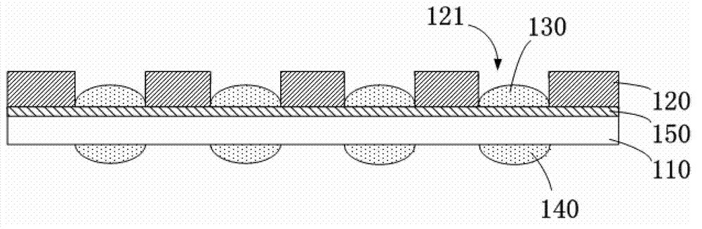
[0071] Please refer to figure 1 , figure 1 It is a schematic diagram of a wafer-level lens module array provided by Embodiment 1 of the present invention. The wafer-level lens module array includes a transparent substrate 110 . The material of the transparent substrate 110 may include but not limited to a transparent glass substrate or a transparent resin substrate, and other materials having corresponding mechanical strength and optical properties and suitable for the manufacturing process of the present invention may also be used to make the transparent substrate 110 . The transparent substrate 110 has a first surface and a second surface, figure 1 Although the first surface and the second surface are not marked in , they can be regarded as corresponding figure 1 The upper surface and the lower surface of the transparent substrate 110.
[0072] Located on the first surface (ie, the upper surface) of the transparent substrate 110 is a through-hole substrate 120 . The mat...
Embodiment 2
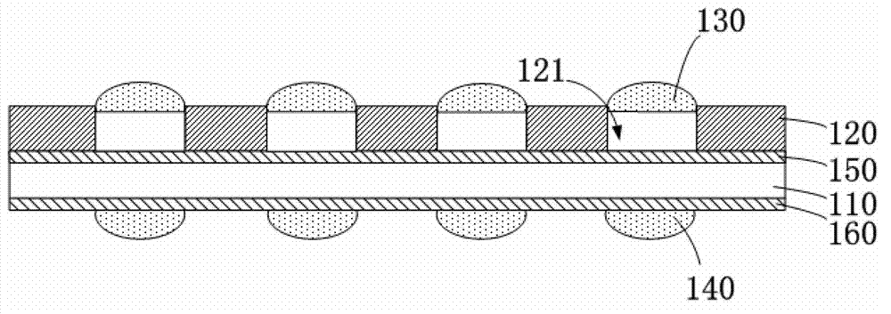
[0079] Please refer to figure 2 , figure 2 It is a schematic diagram of the wafer-level lens module array provided by Embodiment 2 of the present invention. Most of the structure of the wafer-level lens module array provided in this embodiment is the same as that of the wafer-level lens module array described in Embodiment 1. Therefore, this description only describes the differences between the two.
[0080] like figure 2 As shown, in this embodiment, the first lens array is located at the opening of the through hole 121, that is, the first lens array composed of the first lens 130 is not located on the through-hole substrate 120 and the transparent substrate 110 formed by pasting. The bottom of the through hole 121 is located at the opening of the through hole 121 . from figure 2 It can be seen from the figure that each first lens 130 is partially located inside the through hole 121 , so that the first lens 130 can be fixed at the opening of the through hole 121 . T...
Embodiment 3
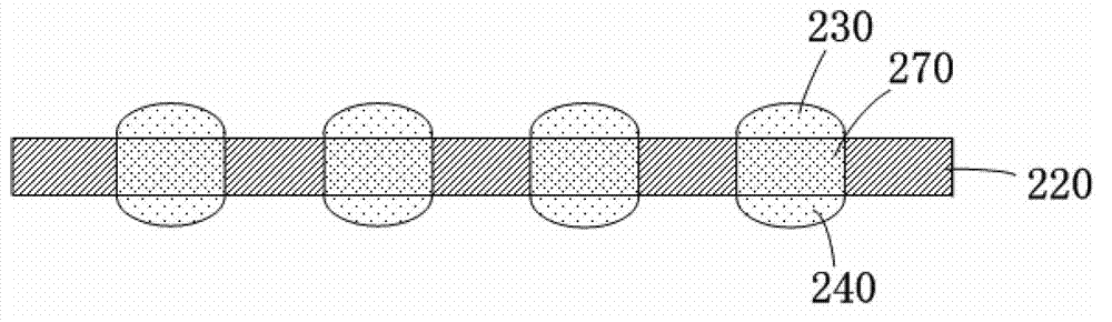
[0083] Please refer to image 3 , image 3 It is a schematic diagram of the wafer-level lens module array provided by Embodiment 3 of the present invention. In this embodiment, the wafer-level lens module array includes a through-hole substrate 220, and the through-hole substrate 220 includes a plurality of through holes 221 ( image 3 The through hole 221 has been filled with a flat filling layer 270, and its structure can be referred to Figure 4 shown). The through-hole substrate 220 in this embodiment is similar to the through-hole substrate 120 in the first embodiment, so its manufacturing material can also be the same as the through-hole substrate 120 in the first embodiment, that is, the through-hole substrate 220 includes but is not limited to BT board, Glass, ceramic or polyimide plates.
[0084] In this embodiment, the wafer-level lens module array also includes at least one of a first lens array and a second lens array, wherein the first lens array is composed o...
PUM
 Abstract
Description
Claims
Application Information
 - Generate Ideas
- Intellectual Property
- Life Sciences
- Materials
- Tech Scout
- Unparalleled Data Quality
- Higher Quality Content
- 60% Fewer Hallucinations
Browse by: Latest US Patents, China's latest patents, Technical Efficacy Thesaurus, Application Domain, Technology Topic, Popular Technical Reports.
© 2025 PatSnap. All rights reserved.Legal|Privacy policy|Modern Slavery Act Transparency Statement|Sitemap|About US| Contact US: help@patsnap.com