

Light emitting diode provided with patterned substrate
A technology of light-emitting diodes and graphics, applied to electrical components, circuits, semiconductor devices, etc., can solve problems such as forward voltage, light intensity, reverse leakage current, wavelength uniformity, etc., to improve wavelength uniformity, improve internal Effect of Quantum Efficiency and Brightness Improvement
- Summary
- Abstract
- Description
- Claims
- Application Information
AI Technical Summary
Problems solved by technology
Method used
Image

Examples
Embodiment 1
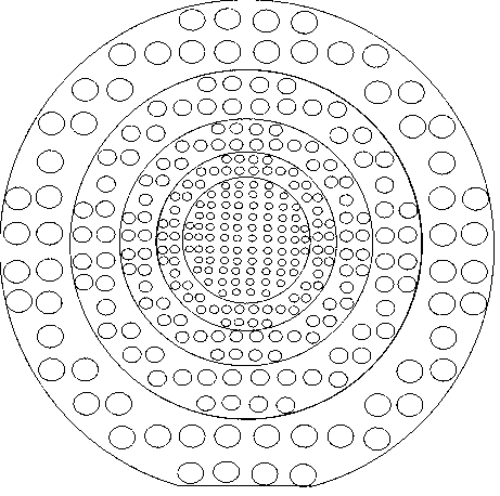
[0021] See attached figure 1 , a light-emitting diode with a patterned substrate, its structure includes a substrate, an N-type semiconductor layer, an active layer and a P-type semiconductor layer. The substrate is divided into 5 concentric ring-shaped areas with the center as the center of the circle, and there are graphics distributed in arrays in the ring-shaped areas; the vertical depth of the graphics is 3 microns, and the cross-section of the graphics is elliptical. The horizontal dimensions are 2, 4, 6, 8, and 10 microns from the inside to the outside, the vertical dimensions are 1.5, 3, 4.5, 6, and 7.5 microns, and the pattern spacing is 4, 8, 12, 16, and 20 microns.
Embodiment 2
[0023] A light-emitting diode with a pattern substrate, its structure includes a substrate, an N-type semiconductor layer, an active layer and a P-type semiconductor layer. The substrate is divided into 6 concentric ring-shaped areas with the center as the center of the circle, and there are graphics distributed in an array in the ring-shaped area; the cross-section of the graphics is elliptical, and the lateral dimensions of the ellipse in the 6 ring-shaped areas are 2 from the inside to the outside. . The order is 0.5, 0.6, 0.7, 0.8, 0.9, 1 micron.
Embodiment 3
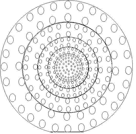
[0025] A light-emitting diode with a pattern substrate, its structure includes a substrate, an N-type semiconductor layer, an active layer and a P-type semiconductor layer. The substrate is divided into 5 concentric ring-shaped areas with the center as the center of the circle. There are graphics distributed in an array in the ring-shaped area; The order is 1, 1.5, 2, 2.5, 3 microns, the pattern spacing is 2, 9, 16, 23, 30 microns, and the vertical depth of the pattern is 0.5, 0.6, 0.7, 0.8, 0.9 microns.
PUM
 Abstract
Description
Claims
Application Information