COB (Chip On Board) packaged LED (Light Emitting Diode) light source and manufacturing method

A technology of LED light source and manufacturing method, which is applied in the direction of electrical components, electric solid devices, circuits, etc., can solve problems such as limitation of luminous angle, product application limitation, small luminous angle and range, etc., so as to improve the luminous angle and luminous range, improve light effect

Inactive Publication Date: 2013-05-01
张刚维 +1
View PDF8 Cites 9 Cited by
  • Summary
  • Abstract
  • Description
  • Claims
  • Application Information

AI Technical Summary

Problems solved by technology

However, whether it is a metal substrate such as an aluminum substrate or a ceramic substrate such as alumina or aluminum nitride, the LED light source manufactured by the COB packaging p

Method used


Image

  • COB (Chip On Board) packaged LED (Light Emitting Diode) light source and manufacturing method
  • COB (Chip On Board) packaged LED (Light Emitting Diode) light source and manufacturing method
  • COB (Chip On Board) packaged LED (Light Emitting Diode) light source and manufacturing method

Examples


Embodiment 1

[0042] As mentioned in the background technology section, COB packaged LED light sources in the prior art all have the problem of small lighting angle and range of the product. Generally, the lighting angle is limited to 120 degrees or less, and the product application is greatly restricted.

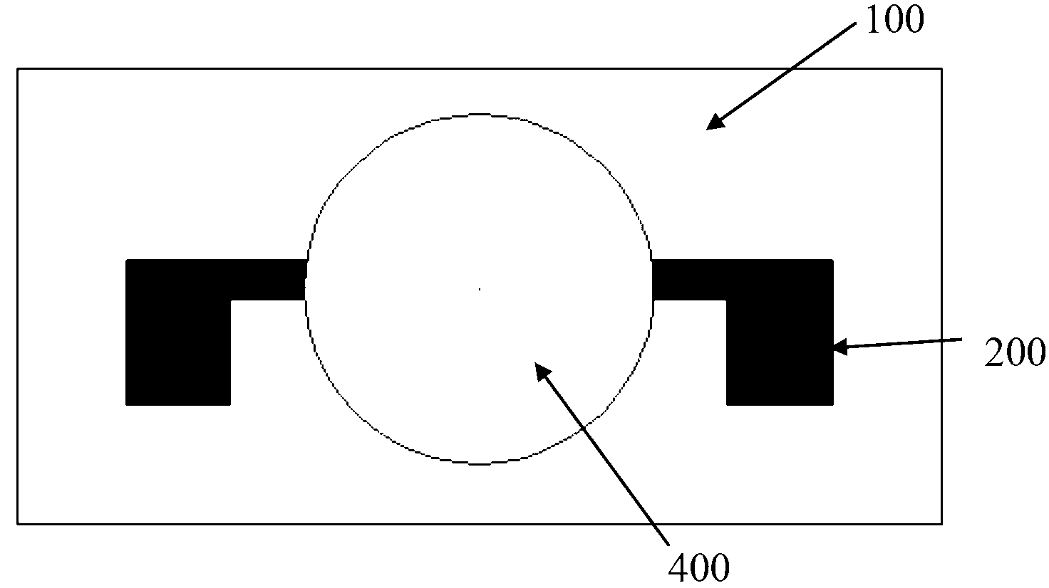
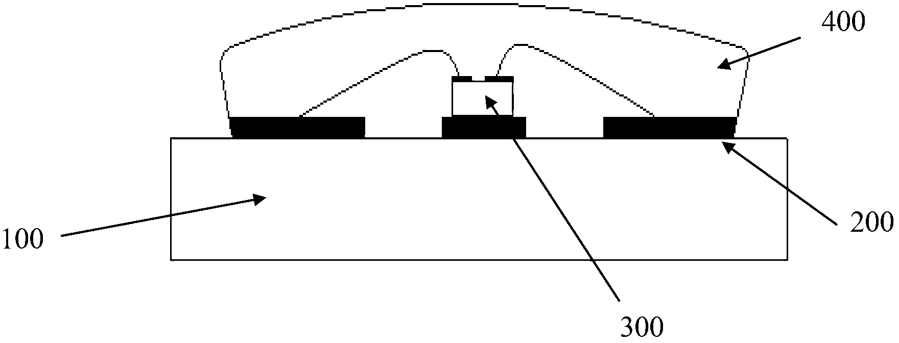
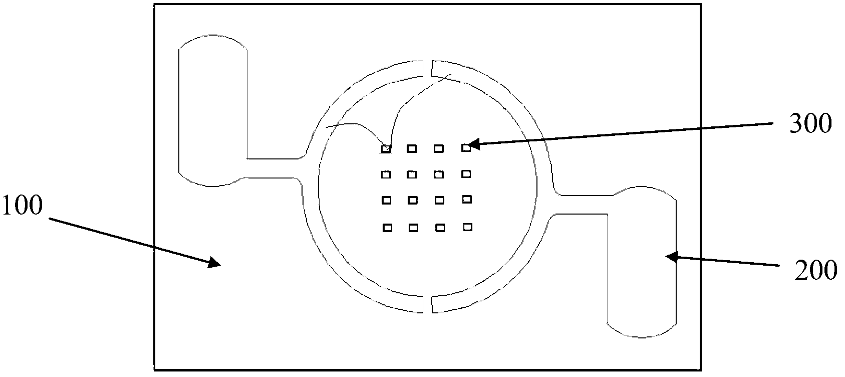
[0043] Based on the above reasons, this embodiment discloses a COB packaged LED light source, the structure of which is as follows Figure 1-Figure 3 as shown, figure 1 For its schematic diagram, figure 2 for its profile, image 3 It is a schematic diagram of the connection between the LED chip and the electrodes. The LED light source includes:

[0044] Substrate 100 , electrodes 200 , LED chips 300 and fluorescent glue 400 ; the front area of ​​the substrate 100 is a device placement area, and the electrodes 200 are arranged on the substrate 100 . The LED chip 300 is arranged on the front of the substrate 100 ; the fluorescent glue 400 covers the surface of the LED chip 300 . Wher...

Embodiment 2

[0061] The difference between this embodiment and the previous embodiment is that in this embodiment, a sapphire substrate is used to make the LED light source. Since the light transmittance of the sapphire material is much higher than 80%, the light efficiency of the light source is as high as 130lm / W or more. Moreover, since the thermal conductivity of the sapphire material reaches 25W / mk, the LED light source made of it dissipates heat quickly during operation, so that the service life of the light source can reach 50,000 hours, and it has higher temperature resistance than traditional aluminum substrates.

Embodiment 3

[0063] The difference between this embodiment and the above-mentioned embodiments is that in this embodiment, a flip-chip connection method is adopted. In this flip-chip connection method, it is necessary to set a part of the electrodes inside the substrate, and this part of the electrodes also includes the positive part and the negative part respectively. The connection method is shown in Figure 5 (B), specifically:

[0064] The two electrodes of the LED chip are directly electrically connected to the corresponding parts of the electrode 200 after reflow soldering with the solder paste. Specifically, the positive part of the LED chip is welded to the positive part of the electrode, and the negative part of the LED chip is welded to the negative part of the electrode.

[0065] This method saves the step of connecting the electrodes through conductive leads. At the same time, most of the light-emitting surface of the flip-chip chip is on the fluorescent glue surface of the ligh...


PUM

PropertyMeasurementUnit
Thermal conductivityaaaaaaaaaa
Light effectaaaaaaaaaa

Abstract

The invention discloses a COB (Chip On Board) packaged LED (Light Emitting Diode) light source. The LED light source comprises a substrate, an electrode, an LED chip and a fluorescent glue, wherein the electrode is arranged on the substrate; the LED chip is arranged on a positive surface of the substrate and is electrically connected with the electrode; the fluorescent glue covers the LED chip; and the substrate is a transparent substrate, and the heat dispersion of the transparent substrate is good. According to the COB packaged LED light source and a manufacturing method thereof provided by the invention, the substrate is changed from an opaque substrate into a cooling transmitting substrate with high efficiency, so that the COB packaged LED light source can shine 360 degrees, an emitting angle and a luminous range of a product are extended, and a lighting effect of the light source is improved. In addition, a substrate material is good in heat dissipation performance and fast in heat dispersion velocity, so that the condition that the fluorescent glue is subjected to aging failure in a high-temperature working environment is avoided, the service life of the fluorescent glue is prolonged, and the thermal resistance and lumens depreciation of the product is reduced. Therefore, the COB packaged LED light source and the manufacturing method can be suitable for a COB packaging technology with high power.

Description

technical field [0001] The invention relates to integrated semiconductor lighting components, in particular to a COB packaged LED light source and a manufacturing method thereof. Background technique [0002] LED (Light Emitting Diode) is a light-emitting semiconductor component. Because of its good controllability, simple structure, small size, pure and rich colors, impact resistance, vibration resistance, and fast response time, it is recognized as the 21st century One of the most promising high-tech products, while triggering the lighting revolution, it also makes a major contribution to promoting energy conservation, emission reduction, and environmental protection. [0003] COB is the English abbreviation of Chip On Boarding (chip on board direct loading), which is a kind of LED chip directly pasted on the PCB (Printed Circuit Board) board by adhesive or solder, and then the chip and the PCB board are realized by wire bonding. Packaging technology for electrical interc...

Claims


Application Information

Patent Timeline
IPC IPC(8): H01L33/58H01L33/64
CPCH01L2224/14H01L2224/16225H01L2224/48091H01L2224/73265H01L2924/00014
Inventor 张刚维张飞林
Owner 张刚维
Why Eureka
Try Eureka