Micro-electromechanical system (MEMS) silicon wafer scribing and cutting and structure releasing method

A silicon wafer, dicing and cutting technology, applied in the direction of microstructure technology, microstructure devices, manufacturing microstructure devices, etc., can solve problems such as edge jumping, silicon chip contamination, large internal stress of chips, etc., and achieve high quality High efficiency, improved production efficiency, and low cost effects

Active Publication Date: 2013-05-08
YANTAI RAYTRON TECH
View PDF11 Cites 19 Cited by
  • Summary
  • Abstract
  • Description
  • Claims
  • Application Information

AI Technical Summary

Problems solved by technology

[0009] The technical problem to be solved by the present invention is to provide a MEMS silicon wafer dicing cutting and structure release method, which overcomes the edge jumping and silicon chip contamination that the scribing process in the prior art is...

Method used

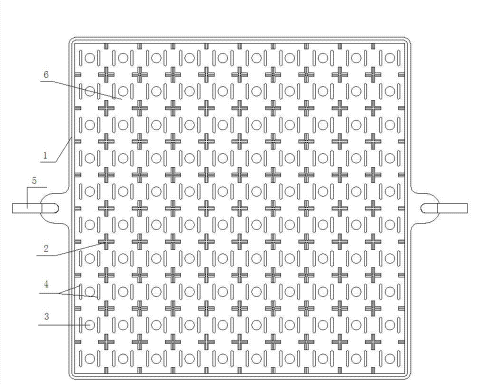
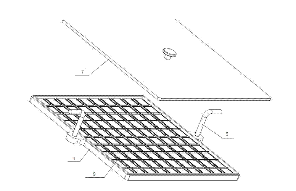
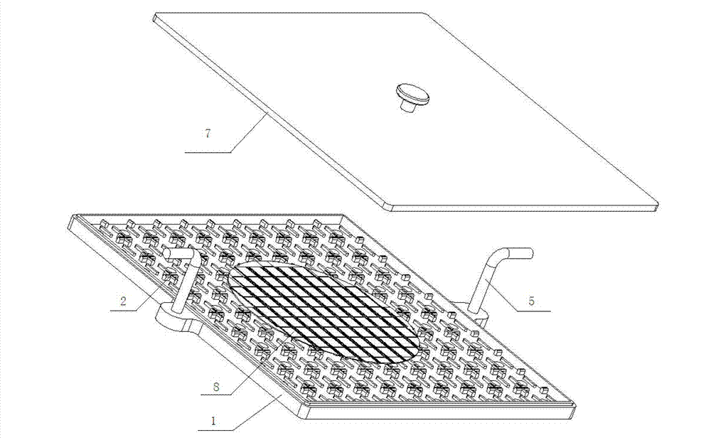

Image

  • Micro-electromechanical system (MEMS) silicon wafer scribing and cutting and structure releasing method
  • Micro-electromechanical system (MEMS) silicon wafer scribing and cutting and structure releasing method
  • Micro-electromechanical system (MEMS) silicon wafer scribing and cutting and structure releasing method

Examples


Embodiment 1

[0041] A MEMS silicon wafer dicing cutting and structure release method, comprising the following steps:

[0042] Step 1: Paste the UV film, paste the UV film on the back of the MEMS silicon wafer; put the front side of the silicon wafer down, the back side up, and put a layer of dust-free filter paper underneath, the size of which is the same as that of the wafer, and place it in the film mounter. right in the middle. Pull out the UV film from the rear reel of the film lamination machine. The length exceeds the patch circular iron ring by 10cm. If the film is partially wrinkled, it needs to be further tightened until the surrounding is even and flat. On the back of the wafer and on the circular iron ring; cut off the UV film beyond the circular iron ring.

[0043] Step 2: For the first scribing, place the silicon wafer with UV film facing up on the scribing table of the dicing machine, set the silicon wafer according to the thickness of the scribing, and set the silicon wafe...

Embodiment 2

[0052] A MEMS silicon wafer dicing cutting and structure release method, comprising the following steps:

[0053] Step 1: Paste the UV film, and paste the UV film on the back of the MEMS silicon wafer; put the front side of the silicon wafer down and the back side up, and put a layer of dust-free filter paper underneath, the size of which is the same as that of the wafer, and place it on the side of the film mounter. right in the middle. Pull out the UV film from the rear reel of the film lamination machine. The length exceeds the patch circular iron ring by 10cm. If the film is partially wrinkled, it needs to be further tightened until the surrounding is even and flat. On the back of the wafer and on the circular iron ring; cut off the UV film beyond the circular iron ring.

[0054] Step 2: For the first scribing, place the silicon wafer with UV film facing up on the scribing table of the dicing machine, set the silicon wafer according to the thickness of the scribing, and s...


PUM

PropertyMeasurementUnit
Heightaaaaaaaaaa
Widthaaaaaaaaaa
Lengthaaaaaaaaaa

Abstract

The invention relates to a micro-electromechanical system (MEMS) silicon wafer scribing and cutting and structure releasing method which comprises the following steps of: attaching an ultraviolet (UV) film to the back of an MEMS silicon wafer; setting a first scribing thickness of the silicon wafer or the height of a scribing cutter, wherein the first scribing thickness is 40-55 percent of that of the silicon wafer; setting a second scribing thickness to be thickness of residual silicon (full scribing) of the silicon wafer or setting the height of the scribing cutter to be a sum of the thickness of the residual silicon to be finally retained and the thickness of the UV film (semi scribing); after scribing is finished, eliminating 80-90 percent of the viscosity of the UV film; picking up a chip on the UV film or taking down the whole silicon wafer and putting the silicon wafer into a tray with filtration holes; putting the tray into a degummin solution for degumming; eliminating liquid and dehydrating; and releasing the structure. By a twice scribing technology, the problems that the edge of the thick chip is hopped, pollution is caused by silicon slag, and inner stress on the chip is large because of scribing are solved; and meanwhile, by the designed special tray, the sequence contradiction of MEMS silicon wafer scribing and structure releasing is avoided.

Description

technical field [0001] The invention relates to a MEMS silicon wafer dicing cutting and structure releasing method, which belongs to micro-processing of micro-electromechanical systems and wafer dicing and cutting methods. Background technique [0002] Micro-electromechanical systems (MEMS, Micro-electromechanical Systems) is a high-tech field based on microelectronics technology and micro-processing technology. MEMS technology can integrate mechanical components, drive components, electronic control systems, digital processing systems, etc. into an integral micro-unit. MEMS devices have many advantages such as tiny, intelligent, executable, integrable, good process compatibility, and low cost. The development of MEMS technology has opened up a new technical field and industry. Micro sensors, micro actuators, micro components, micro mechanical optical devices, vacuum microelectronic devices, power electronic devices, etc. made by MEMS technology are widely used in aviation,...

Claims


Application Information

Patent Timeline
IPC IPC(8): B81C1/00
Inventor 甘先锋杨水长王宏臣孙瑞山
Owner YANTAI RAYTRON TECH
Why Eureka
Try Eureka