
Method for preparing nano-array patterns by icp etching gan-based multiple quantum wells

A nano-array and nano-pattern technology, applied in electrical components, circuits, semiconductor devices, etc., can solve problems such as substrate material and structural damage, and achieve the effects of reducing etching, reducing losses, and promoting chemical reactions.

Inactive Publication Date: 2015-11-18
NANJING UNIV
View PDF5 Cites 0 Cited by
  • Summary
  • Abstract
  • Description
  • Claims
  • Application Information

AI Technical Summary

Problems solved by technology

There are complex chemical and physical processes in the ICP etching process. The physical action will cause great damage to the substrate material and structure, and the defect of the chemical process is that the etching is isotropic.

Method used


Image

  • Method for preparing nano-array patterns by icp etching gan-based multiple quantum wells
  • Method for preparing nano-array patterns by icp etching gan-based multiple quantum wells
  • Method for preparing nano-array patterns by icp etching gan-based multiple quantum wells

Examples


Embodiment

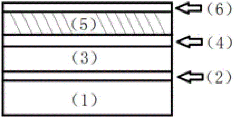
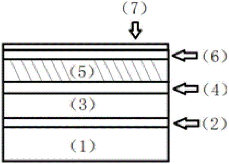
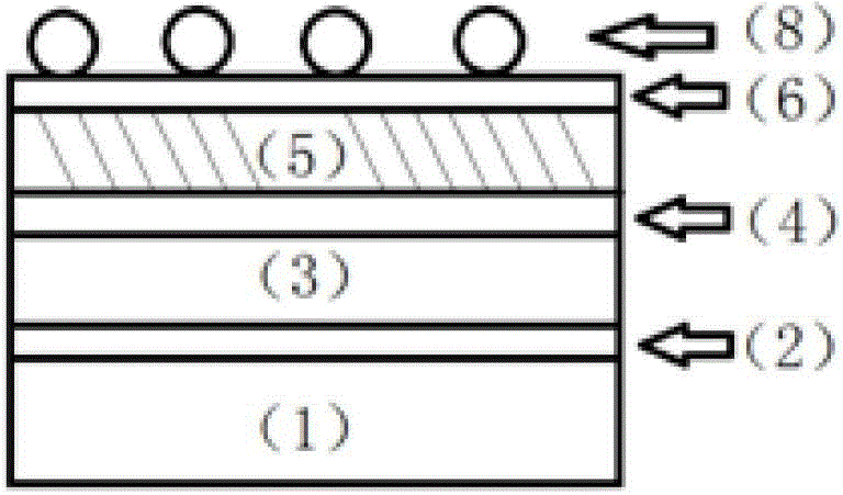
[0063] refer to Figure 1-Figure 5 As shown, the present invention provides a GaN-based multi-quantum well nanometer light-emitting array device, comprising the following steps:

[0064] Step 1: Take a sapphire substrate 1 with a thickness of 300um.

[0065]Step 2: epitaxially grow a GaN buffer layer 2 with a thickness of 30nm, a non-doped GaN layer 3 with a thickness of 2um, an n-type GaN layer 4 with a thickness of 500nm, and an InGaN / GaN quantum well layer with a thickness of 100nm on a sapphire substrate 1 by ThomasSwan MOCVD and a 200nm thick p-type GaN layer 6, wherein the InGaN / GaN quantum well layer 5 is alternately grown indium gallium nitride / gallium nitride, the entire thickness is about 100nm, the period number is 5, and the In composition is 0.18. Ga source, In source and N source are trimethyl gallium, trimethyl indium and liquid ammonia (blue ammonia) respectively.

[0066] Step 3: Carry out PVD vacuum evaporation of Ni metal on the p-type GaN layer 6 using PV...


PUM

PropertyMeasurementUnit
sizeaaaaaaaaaa
thicknessaaaaaaaaaa
thicknessaaaaaaaaaa

Abstract

A preparation method of a nano array pattern through inductive coupling plasma (ICP) GaN-based multiple quantum wells includes the following steps: taking a substrate made of silicon or sapphire or gallium nitride, sequentially growing a GaN buffering layer, an n-type GaN layer, an InGaN / GaN quantum well layer and P-type GaN on the substrate in an epitaxial mode, forming a primary GaN substrate, wherein the thickness of the whole quantum well layer is about 50nm-200nm, and periodicity of the whole quantum well layer is 2-10, carrying out vacuum evaporation on a metal layer through physical vapor deposition (PVD) on the GaN substrate, carrying out high-temperature anneal on the substrate of the metal layer grown due to the vacuum evaporation, utilizing ICP etching process, etching the GaN substrate to the n-type GaN layer or a part of the n-type GaN layer, and forming an InGan / GaN nano column.

Description

technical field [0001] The invention relates to the field of photoelectric devices, in particular to ICP etching GaN-based multi-quantum wells to prepare nanometer array patterns. Background technique [0002] Group III nitride materials, because of their continuously adjustable bandgap from 0.7ev to 6.2ev, combined with the advantages of direct bandgap and optoelectronic applications, make them the best choice for the development of near-infrared-visible-ultraviolet band semiconductor optoelectronic devices. One of the best materials. In recent years, with the extensive research and application of gallium nitride materials, the preparation technology of blue-violet light-emitting diodes (LEDs) and high-mobility transistor materials has been relatively mature, and the third-generation GaN-based semiconductor materials and devices have gradually moved towards industrialization 【1、2、3】 . However, gallium nitride light-emitting diodes are currently facing many problems. For ...

Claims


Application Information

Patent Timeline
Patent Type & Authority Patents(China)
IPC IPC(8): H01L33/06H01L33/00
Inventor 张荣智婷陶涛谢自力万图图叶展圻刘斌修向前李毅韩平施毅郑有炓
Owner NANJING UNIV
Learn More