Programmable polycrystalline silicon fuse device structure and realizing method of technology of programmable polycrystalline silicon fuse device structure

A polysilicon fuse and device structure technology, which is applied in the fields of electric solid device, semiconductor device, semiconductor/solid state device manufacturing, etc., can solve the problems of low integration of polysilicon fuse devices, inability to provide high programming voltage, and low integration, etc. Achieve obvious cost advantages, reduce costs, and improve the effect of integration

Inactive Publication Date: 2013-05-15
SHANGHAI HUAHONG GRACE SEMICON MFG CORP
View PDF4 Cites 7 Cited by
  • Summary
  • Abstract
  • Description
  • Claims
  • Application Information

AI Technical Summary

Problems solved by technology

This feature determines that the integration level of polysilicon fuse devices is very low, which includes the large distance between two polysilicon fuse devices, and the distance between other devices and polysilicon fuse devices.
[0004] With the development of process technology, the line width of semiconductor devices has become smaller, and the integration of devices has become very high. The disadvantages of low integration of traditional polysilicon fuse devices have become more and more obvious. Below 0.25μm process, it is used Metal fuse devices are gradually replaced, but the expensive laser cutting machine required for metal fuse devices makes the cost of this device application much higher
In addition, the high programming voltage of traditional polysilicon fuse devices cannot be provided by advanced technology

Method used


Image

  • Programmable polycrystalline silicon fuse device structure and realizing method of technology of programmable polycrystalline silicon fuse device structure
  • Programmable polycrystalline silicon fuse device structure and realizing method of technology of programmable polycrystalline silicon fuse device structure
  • Programmable polycrystalline silicon fuse device structure and realizing method of technology of programmable polycrystalline silicon fuse device structure

Examples


Embodiment Construction

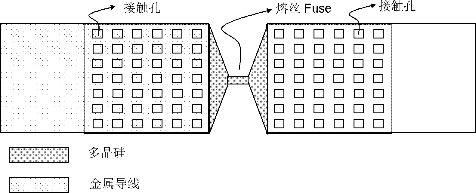
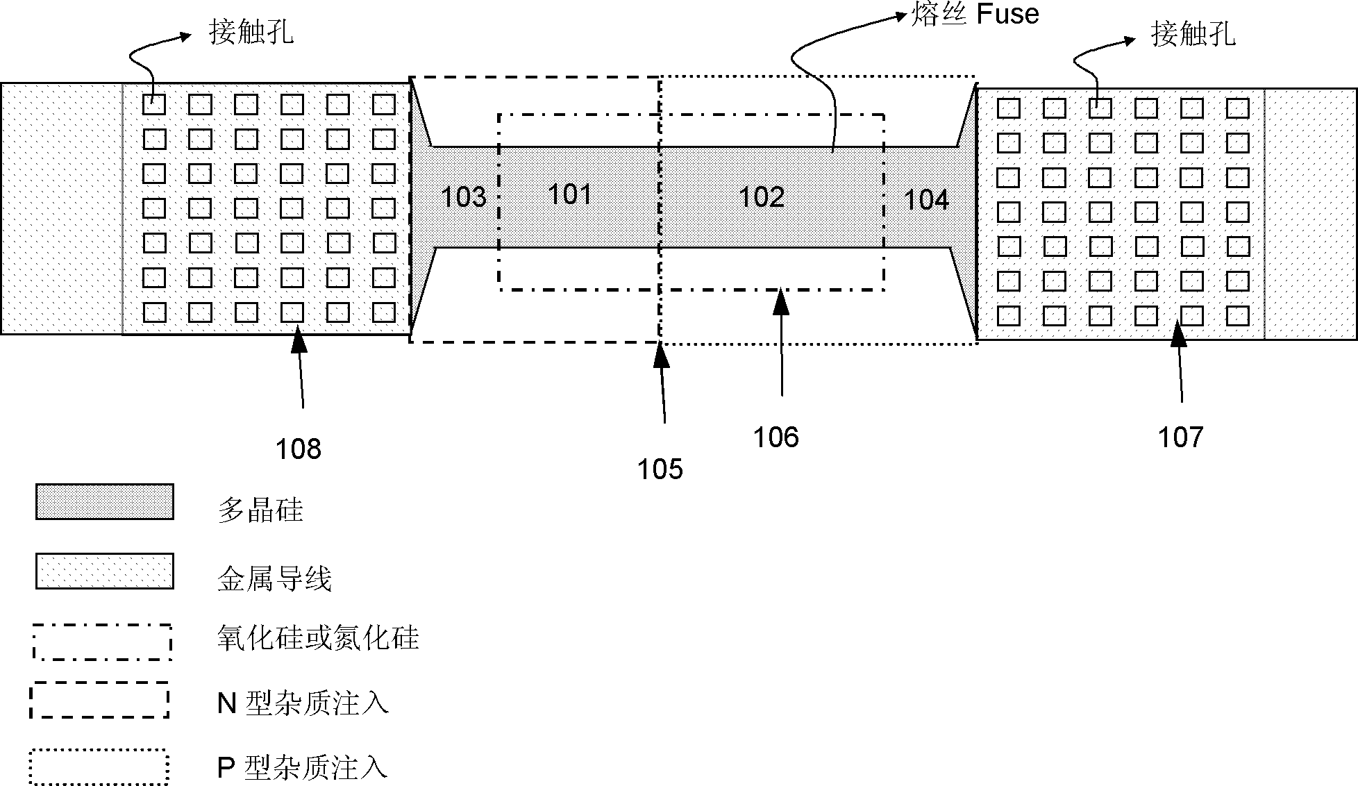
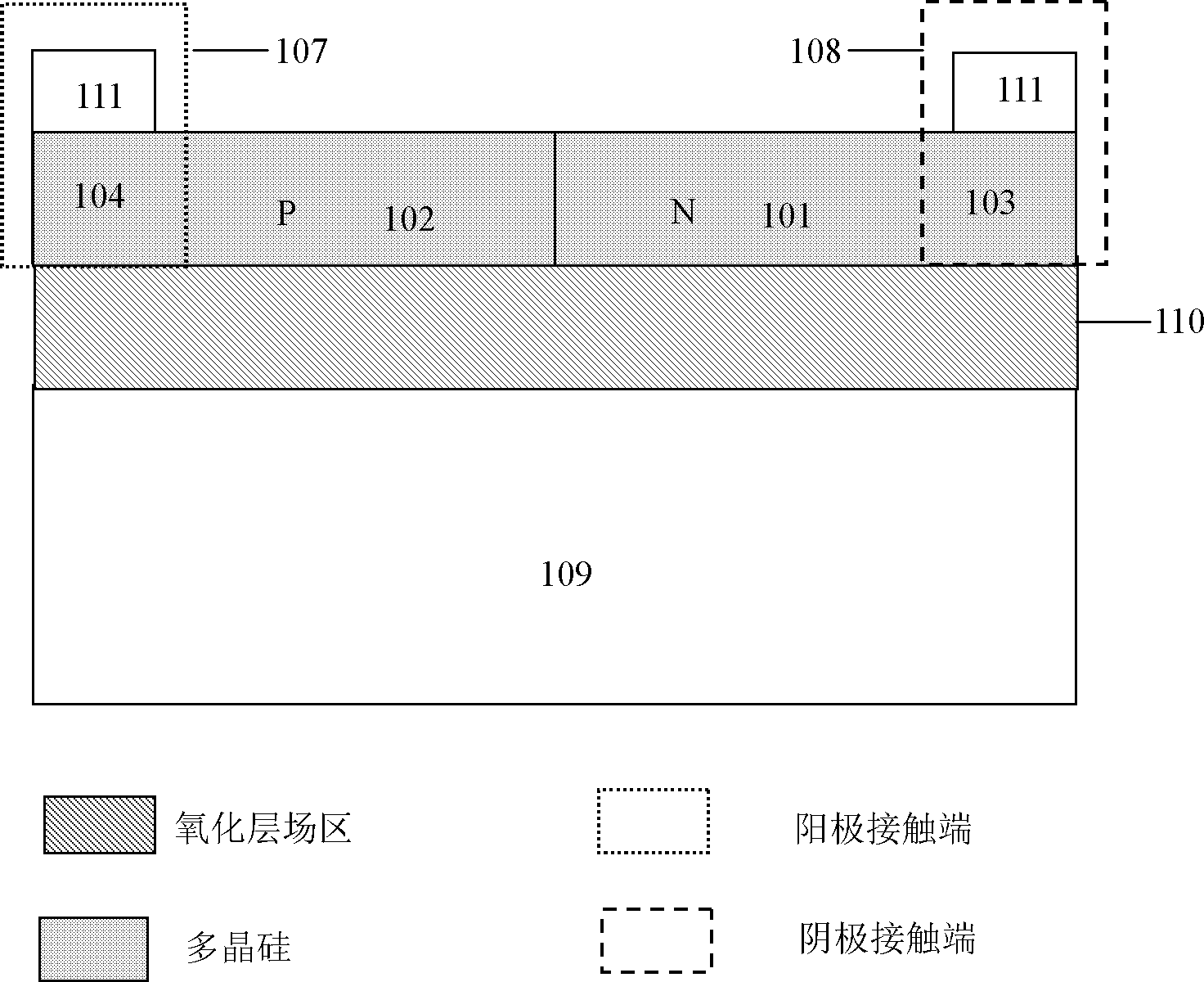
[0039] The programmable polysilicon fuse device structure of the present invention, as figure 2 shown, including:

[0040] N-type high-resistance polysilicon resistance 101 is composed of polysilicon and N-type impurity implantation, and its resistance is 2-3Kohm; there is no metal silicide 111 on the polysilicon, because silicon oxide or silicon nitride 106 is used on the polysilicon The process of forming the metal silicide 111 acts as a protective layer to prevent the formation of metal silicide on the polysilicon, so as to achieve the purpose of forming an N-type polysilicon resistor with a high resistance value;

[0041] P-type high-resistance polysilicon resistor 102 is composed of polysilicon and P-type impurity implantation, and its resistance is 2-3Kohm; there is no metal silicide 111 on the polysilicon, because silicon oxide or silicon nitride 106 is used on the polysilicon The process of forming the metal silicide 111 acts as a protective layer to prevent the form...


PUM

PropertyMeasurementUnit
thicknessaaaaaaaaaa
thicknessaaaaaaaaaa

Abstract

The invention discloses a programmable polycrystalline silicon fuse device structure and a realizing method of the technology of the programmable polycrystalline silicon fuse device structure. The programmable polycrystalline silicon fuse device structure comprises an N type high-resistance polycrystalline silicon resistor, a P type high-resistance polycrystalline silicon resistor an NP diode, a negative electrode contact end and a positive electrode contact end. The method comprises the steps that an oxide layer field area is formed on a P type substrate, a polycrystalline silicon area is formed on the oxide layer field area, P type polycrystalline silicon is formed on one side of the polycrystalline silicon area and N type polycrystalline silicon is formed on the other side of the polycrystalline silicon area, the NP diode is formed in a junction position of the N type polycrystalline silicon and the P type polycrystalline silicon, silicon oxide or silicon nitride is produced in a P,N type high-resistance polycrystalline silicon resistor area to prevent formation of metal silicide, the metal silicide is formed in a P type low-resistance polycrystalline silicon resistor area on the polycrystalline silicon and in an type type low-resistance polycrystalline silicon resistor area on the polycrystalline silicon, a through hole is formed, metal wire connection is achieved, and the negative electrode end and the positive electrode end of a polycrystalline silicon fuse device are led out. The programmable polycrystalline silicon fuse device structure and the realizing method of the technology of the programmable polycrystalline silicon fuse device structure can be applied to various technologies, reliability is guaranteed, the yield of a device is well guaranteed.

Description

technical field [0001] The invention relates to a polysilicon fuse device, in particular to a programmable polysilicon fuse device structure and a process realization method thereof. Background technique [0002] Polysilicon fuse devices are widely used in integrated circuits to perform various functions. For example, redundant storage units are adjusted in SRAM to improve the product yield of SRAM, the frequency of crystal oscillator is adjusted, input / output interfaces are selected for specific applications, and so on. [0003] The traditional polysilicon fuse device requires a relatively high programming voltage to physically fuse the polysilicon, so as to realize the function of device resistance change before and after programming. like figure 1 As shown in the traditional polysilicon fuse device, when the device is programmed, when a large current flows through the fuse part, the huge heat generated will blow the fuse. This process will generate a lot of heat, and th...

Claims


Application Information

Patent Timeline
Patent Type & Authority Applications(China)
IPC IPC(8): H01L23/525H01L21/768
Inventor 仲志华
Owner SHANGHAI HUAHONG GRACE SEMICON MFG CORP
Why Eureka
Try Eureka