Manufacturing method and manufacturing device of flexible printed circuit

A flexible printed circuit and manufacturing device technology, applied in the direction of conductive pattern formation, etc., to achieve the effect of increasing density, high-quality flexible circuit manufacturing, and avoiding porous and loose structures

Active Publication Date: 2013-05-15
SUZHOU INST OF NANO TECH & NANO BIONICS CHINESE ACEDEMY OF SCI
View PDF4 Cites 20 Cited by
  • Summary
  • Abstract
  • Description
  • Claims
  • Application Information

AI Technical Summary

Problems solved by technology

However, the metal film formed by sintering is a porous loose structure, and its bonding force, conductivity, and metal film density cannot be compared with calendered or electrolytic metal foil.

Method used


Image

  • Manufacturing method and manufacturing device of flexible printed circuit
  • Manufacturing method and manufacturing device of flexible printed circuit
  • Manufacturing method and manufacturing device of flexible printed circuit

Examples


Embodiment Construction

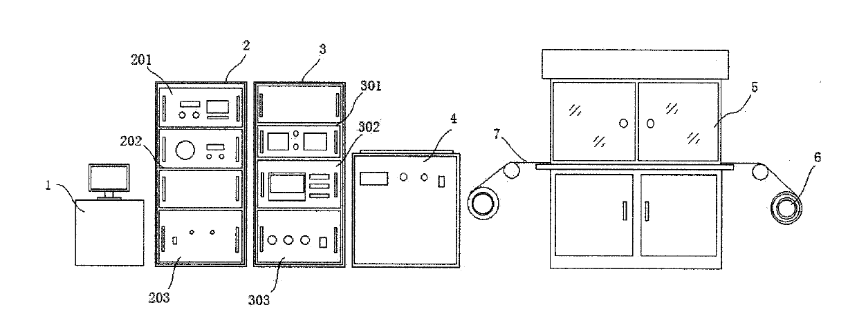
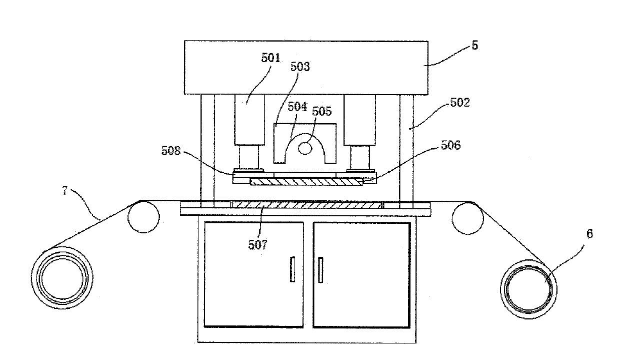
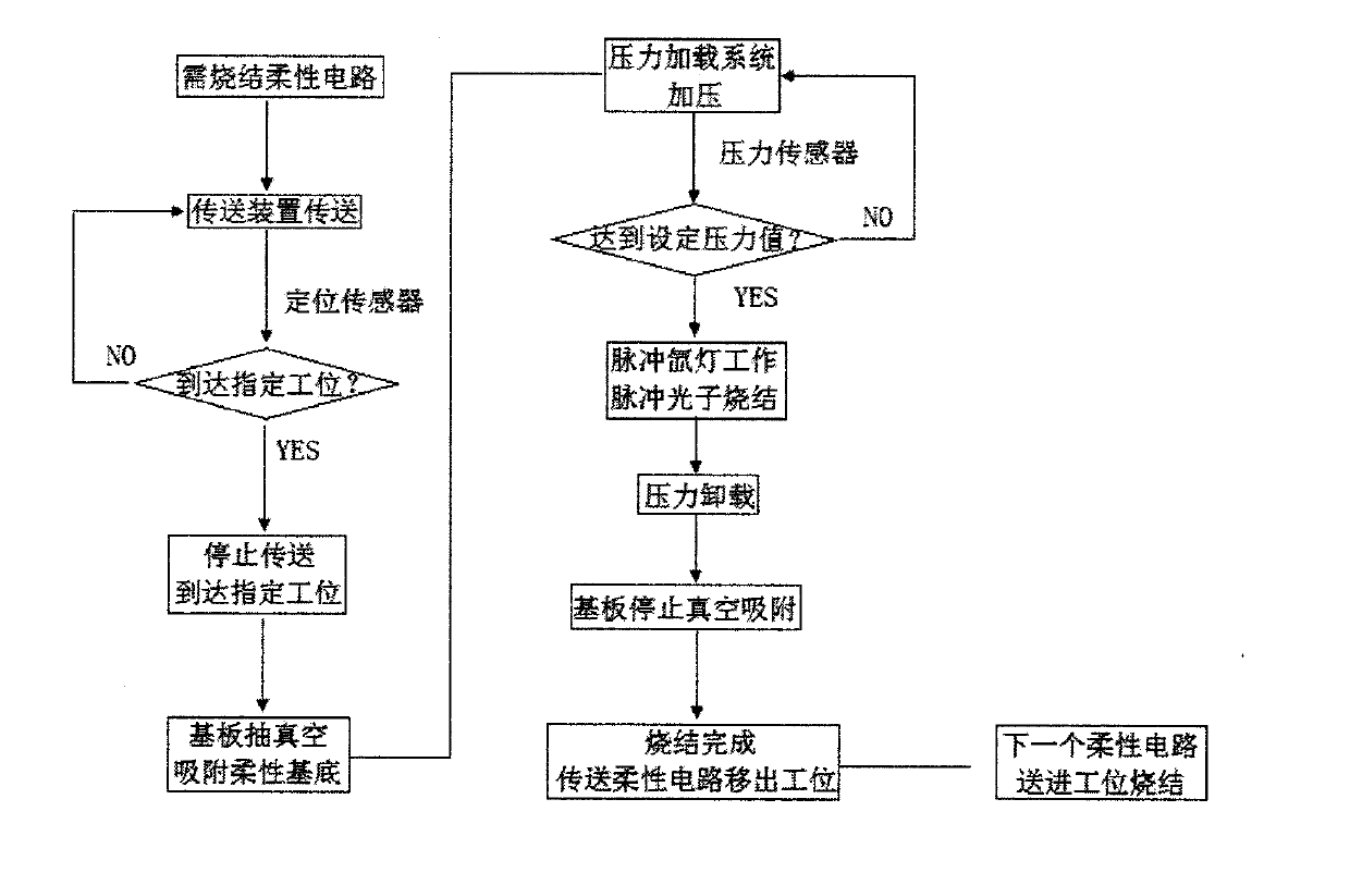
[0032] As mentioned above, in the existing manufacturing process of flexible printed circuit, there are still many deficiencies in the nanoparticle conductive ink sintering technology. technology, a method for manufacturing a flexible printed circuit is proposed, which includes the following steps: providing a patterned flexible printed circuit substrate coated with nano-conductive ink; applying pressure to the upper surface of the flexible printed circuit substrate; The flexible printed circuit substrate is sintered by a xenon lamp sintering process while under pressure to obtain a flexible printed circuit.

[0033] Wherein, according to different choices of materials of the flexible printed circuit substrate, the method of applying pressure to the flexible printed circuit substrate can be a constant pressure method or a variable pressure method; the applied pressure can be selected within the range of 0-40MPa.

[0034] Wherein, the nano-particles in the nano-conductive ink o...


PUM


Abstract

The invention discloses a manufacturing method and a manufacturing device of a flexible printed circuit. The method mainly includes the steps of providing an imaging flexible printed circuit substrate which is coated with nanometer conductive ink or sizing agents; exerting pressure to the flexible printed circuit substrate; and sintering the flexible printed circuit substrate by using xenon lamp sintering technology at the same time when the pressure is exerted and obtaining a target product. By means of the method, a printed circuit can be rapidly manufactured on a low temperature flexible substrate, a metal film which is good in binding force, electrical conductivity and compactness can be obtained, and manufacturing cost is low. The method avoids the processes such as photoetching in the manufacturing process of a traditional flexible printed circuit, rapid and pollution-free flexible printed circuit manufacturing is achieved, and the method is suitable for the production and the manufacture of the flexible printed circuit of the low temperature substrate.

Description

technical field [0001] The invention relates to sintering technology and belongs to the field of material sintering technology, in particular to a method for manufacturing a flexible printed circuit and a manufacturing device thereof. Background technique [0002] In the electronics industry, with the rapid development of modern consumer electronics and miniaturized equipment, flexible printed circuits (FPCBs) are increasingly used due to their advantages such as light weight, thin thickness, small size, high density, and flexibility. Used in mobile phones, notebook computers, digital cameras, liquid crystal displays and other electronic products. Moreover, the number of its use is also increasing. In the traditional mobile phone, about 3-5 pieces are needed, and in the smart mobile phone, it is greatly increased to 7-10 pieces, and the iPAD and other products launched by Apple are as high as 15 pieces. According to the latest statistics released by Taiwan Printed Circuit ...

Claims


Application Information

Patent Timeline
Patent Type & Authority Applications(China)
IPC IPC(8): H05K3/10
Inventor 顾唯兵陈征崔铮
Owner SUZHOU INST OF NANO TECH & NANO BIONICS CHINESE ACEDEMY OF SCI
Why Eureka
Try Eureka