Method for growing thick gate oxide layer for high-voltage metal oxide semiconductor (MOS) device

A technology of oxide semiconductors and high-voltage devices, which is applied in the direction of semiconductor devices, can solve problems such as high risk and complex process, and achieve the effects of reducing risk, simple process, and avoiding changes in electrical characteristics and reliability performance

Active Publication Date: 2013-06-05
SHANGHAI HUAHONG GRACE SEMICON MFG CORP
View PDF3 Cites 3 Cited by
  • Summary
  • Abstract
  • Description
  • Claims
  • Application Information

AI Technical Summary

Problems solved by technology

In this way, there are disadvantag

Method used


Image

  • Method for growing thick gate oxide layer for high-voltage metal oxide semiconductor (MOS) device
  • Method for growing thick gate oxide layer for high-voltage metal oxide semiconductor (MOS) device
  • Method for growing thick gate oxide layer for high-voltage metal oxide semiconductor (MOS) device

Examples


Embodiment Construction

[0037] The present invention proposes for the first time that the growth of the thick gate oxide layer of the high-voltage device occurs before the shallow trench isolation (STI), and the silicon nitride layer is used as a hard mask to ensure the thickness of the thick gate oxide layer. The method can avoid changes in the electrical characteristics and reliability performance of low-voltage devices and non-volatile memory devices during the high-voltage gate oxidation process, reduce risks, and at the same time, the process is simple and the number of photolithographic plates remains unchanged. The specific process is as follows:

[0038] Protection of thick gate oxide growth for high-voltage devices occurs prior to shallow trench isolation (STI) formation, through silicon nitride layers as hard masks associated with the process flow. details as follows:

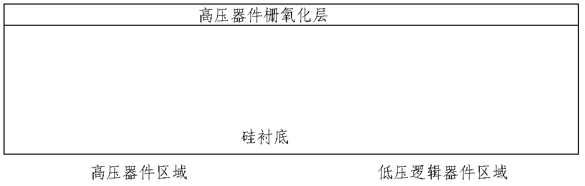
[0039] (1) if figure 1 As shown, thick gate oxide (SiO2①) growth for high-voltage devices.

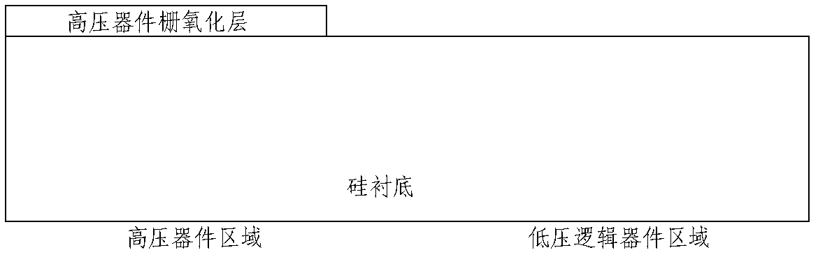
[0040] (2) if figure 2 A...


PUM


Abstract

The invention discloses a method for growing a thick gate oxide layer for a high-voltage MOS device. The growth of the thick gate oxide layer for the high-voltage device happens before shallow channel isolation, and a silicon nitride layer serves as a hard mask. According to the method, changes of electrical characteristics and reliability of low-voltage devices in a high-voltage gate oxidation process are avoided, risks are reduced; and simultaneously, the process is simple, and the number of photoetching plates remains unchanged.

Description

technical field [0001] The present invention relates to integrated circuit manufacturing technology. Background technique [0002] With the development of integrated circuits, single-chip system integration has become a trend. This requires both the intelligent control circuit of the MCU and the analog or high-voltage circuit on one chip. [0003] However, in the actual process, the growth of a thick gate oxide layer for high-voltage devices will introduce additional high-temperature and long-term thermal processes and wet etching processes, resulting in changes in related particle injection conditions and lattice defects induced by stress changes in the silicon substrate. And surface silicon consumption, which causes serious changes in the electrical characteristics and reliability performance of low-voltage devices. Existing solutions have focused on growing thick gate oxides for high-voltage devices after shallow trench isolation (STI) and before gate oxide growth for l...

Claims


Application Information

Patent Timeline
IPC IPC(8): H01L21/28
Inventor 刘剑陈瑜陈华伦
Owner SHANGHAI HUAHONG GRACE SEMICON MFG CORP
Why Eureka
Try Eureka