Method for manufacturing insulated gate bipolar transistor (IGBT) component combined with fast recovery diode (FRD)

A device manufacturing method and multiple tube technology, applied in semiconductor/solid-state device manufacturing, electrical components, circuits, etc., can solve the problems of large occupied area, large on-state voltage, high base resistance, etc. The effect of small state resistance and short fall delay time

Active Publication Date: 2013-06-05
SHANGHAI HUAHONG GRACE SEMICON MFG CORP
View PDF3 Cites 26 Cited by
  • Summary
  • Abstract
  • Description
  • Claims
  • Application Information

AI Technical Summary

Problems solved by technology

Although the withstand voltage is enough, but the base resistance is high, the Joule heat will be larger in the on-state, and the on-state voltage will be larger in

Method used


Image

  • Method for manufacturing insulated gate bipolar transistor (IGBT) component combined with fast recovery diode (FRD)
  • Method for manufacturing insulated gate bipolar transistor (IGBT) component combined with fast recovery diode (FRD)
  • Method for manufacturing insulated gate bipolar transistor (IGBT) component combined with fast recovery diode (FRD)

Examples


Example Embodiment

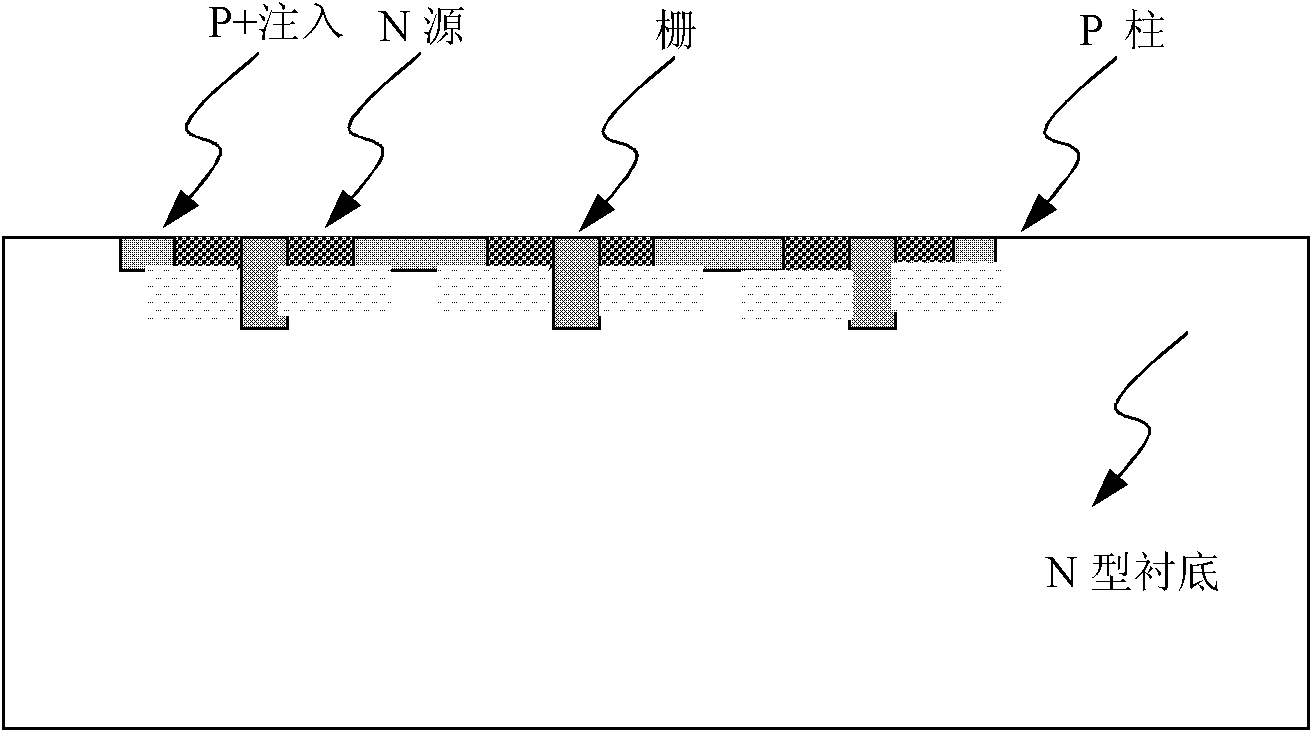
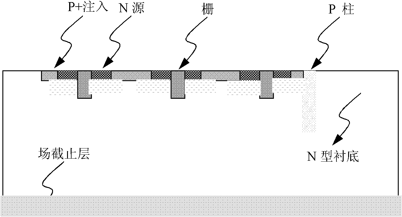
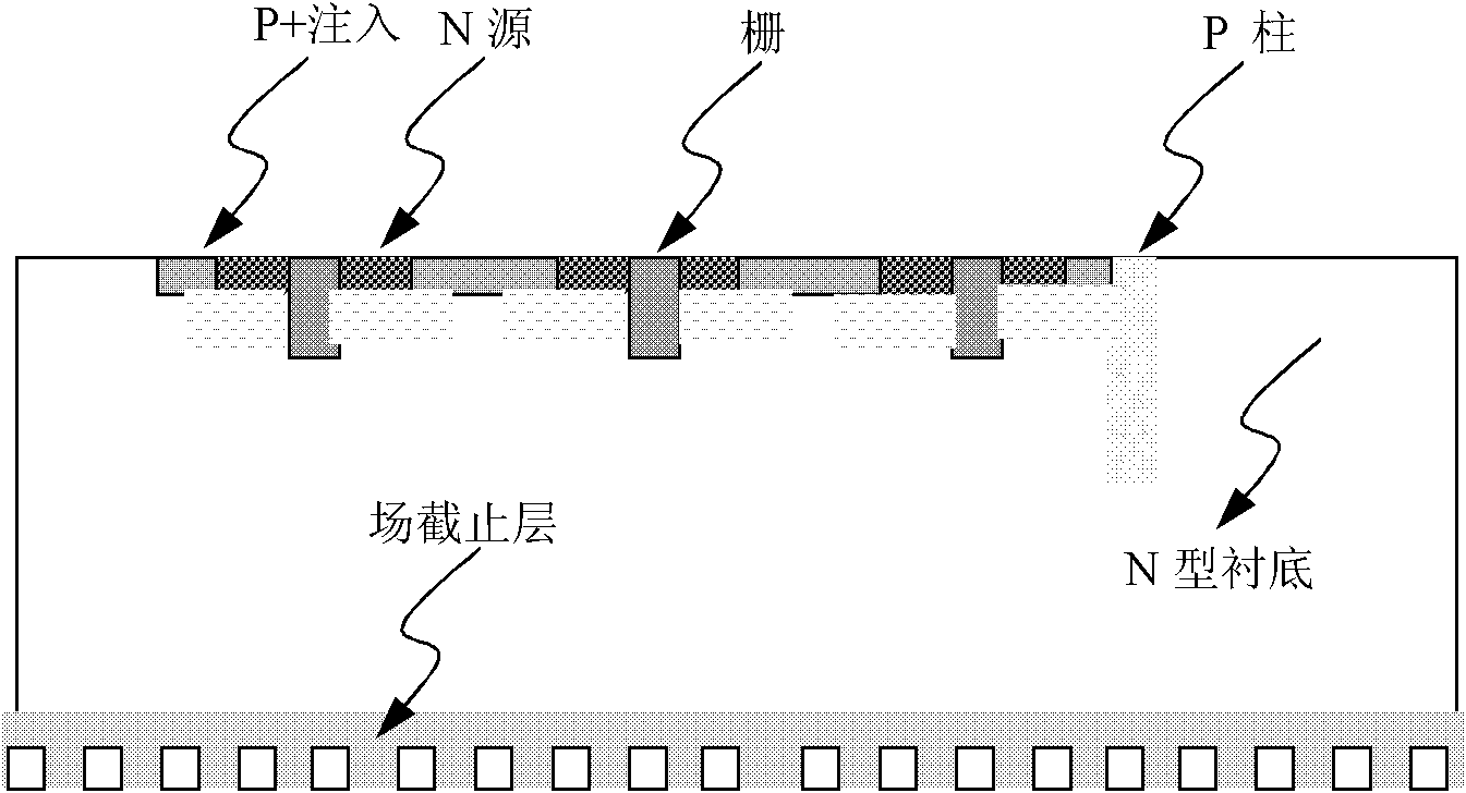
[0023] The present invention provides a special 8-inch device structure combined with a Fly-Trench trench field-stop insulated gate bipolar transistor IGBT. After the device is completed with an insulated gate bipolar transistor IGBT in the usual sense, it is then performed on the back side. The implantation of the field stop layer and the high temperature and long time push well to form the field stop layer, and then lithographically define the back side, trench trenches on the reverse side to grow highly doped polysilicon to form a reverse current path, and then the back side is injected and activated by the collector. And the extraction of the back metal to form the back collector.

[0024] The function of the present invention is to form the backside reverse voltage path by filling the backside trenches with N-type polysilicon, without worrying about the activation rate of N-type P ions, so that the process cost is greatly saved, and RC is integrated in the insulated gate bipo...


PUM

PropertyMeasurementUnit
Thicknessaaaaaaaaaa
Widthaaaaaaaaaa
Thicknessaaaaaaaaaa

Abstract

The invention discloses a method for manufacturing an insulated gate bipolar transistor (IGBT) component combined with a fast recovery diode (FRD). The method comprises the steps of defining exposure of a trench gate, growing and doping N-type polycrystalline silicon, etching the polycrystalline gate, conducting injection and drive-in to a source and a P trap in the front, reducing silicon slices at the back, conducting the phosphonium ion injection at the back, conducting the phosphonium ion drive-in at the back under a high temperature and for a long time at the back, digging a groove at the back, growing and highly doping N-type polycrystalline silicon in the groove at the back, conducting the collector electrode B injection at the back, and conducting the collector electrode B drive-in and the collector electrode gold evaporation. The IGBT component manufacturing method has a larger substrate concentration of the IGBT component and a lower cost than the prior art. The PNP base width of the IGBT combined with the fast recovery diode is smaller than that of a common IGBT, on-state resistance is smaller, generated joule heat is smaller, dropping detention time is shorter and bearable short-circuit current is larger under the same voltage during off-state.

Description

Technical field [0001] The invention belongs to a method for manufacturing a semiconductor device in a semiconductor device. Background technique [0002] IGBT (Insulated Gate Bipolar Transistor) insulated gate bipolar transistor is a composite fully controlled voltage-driven power semiconductor device composed of BJT (bipolar transistor) and MOS (insulated gate field effect transistor), which also has MOSFET The advantages of high input impedance and low on-voltage drop of GTR. The saturation voltage of GTR is reduced, the current-carrying density is high, but the drive current is large; the MOSFET drive power is small, the switching speed is fast, but the conduction voltage drop is large, and the current-carrying density is small. The insulated gate bipolar transistor IGBT combines the advantages of the above two devices, with low driving power and reduced saturation voltage. It is very suitable to be used in conversion systems with a DC voltage of 600V and above, such as AC ...

Claims


Application Information

Patent Timeline
IPC IPC(8): H01L21/331
Inventor 王海军
Owner SHANGHAI HUAHONG GRACE SEMICON MFG CORP
Why Eureka
Try Eureka