Method of manufacturing field termination type insulated gate bipolar translator (IGBT) component in patching mode

A technology for manufacturing fields and devices, applied in semiconductor/solid-state device manufacturing, electrical components, circuits, etc., can solve the problems of broken, large silicon wafers, increased costs, etc., and achieve the effect of reducing the probability of fragmentation and saving huge costs

Inactive Publication Date: 2013-06-05
SHANGHAI HUAHONG GRACE SEMICON MFG CORP
View PDF9 Cites 11 Cited by
  • Summary
  • Abstract
  • Description
  • Claims
  • Application Information

AI Technical Summary

Problems solved by technology

[0011] The general-purpose equipment of semiconductor manufacturers is used to process silicon wafers with a standard thickness (generally 725 μm), and there is a greater risk of silicon

Method used


Image

  • Method of manufacturing field termination type insulated gate bipolar translator (IGBT) component in patching mode
  • Method of manufacturing field termination type insulated gate bipolar translator (IGBT) component in patching mode
  • Method of manufacturing field termination type insulated gate bipolar translator (IGBT) component in patching mode

Examples


no. 1 example

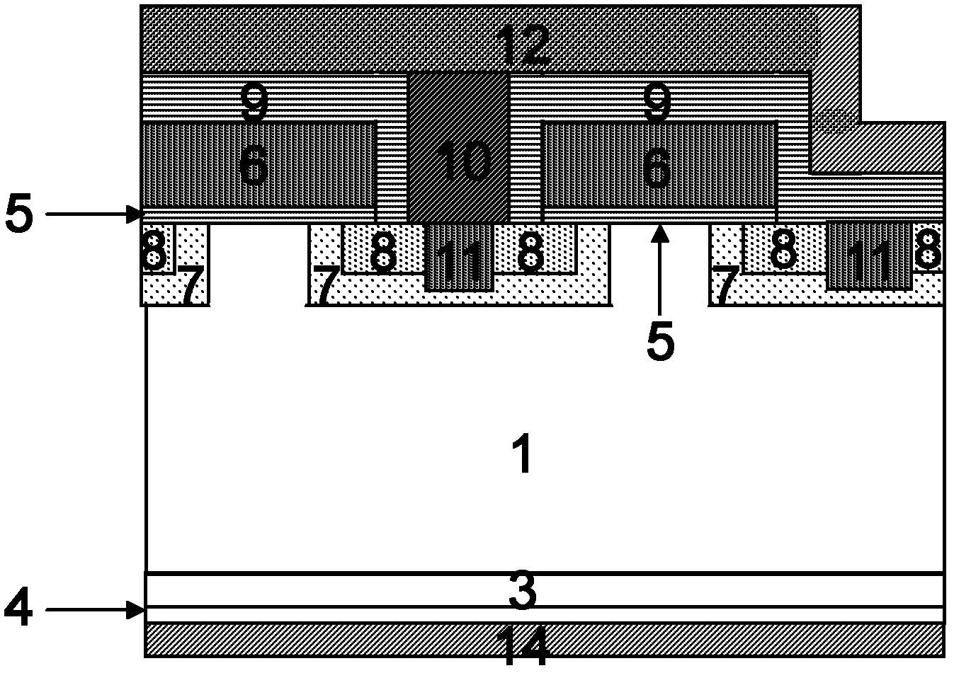
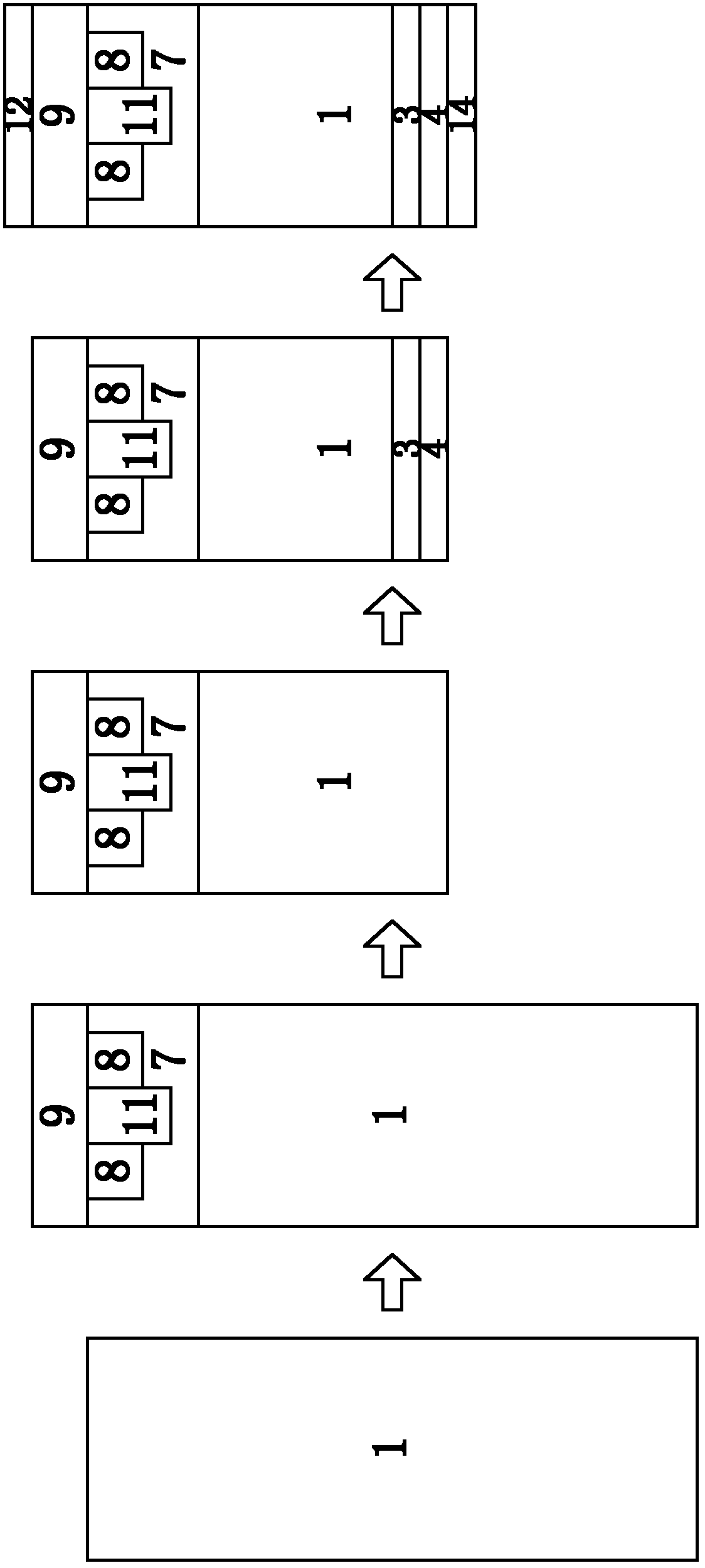
[0024] see image 3 , which is the first embodiment of the method for manufacturing a field-stop type IGBT device in the patch mode of the present invention, which includes the following steps:

[0025] In the first step, the first silicon substrate 10 and the second silicon substrate 40 are selected, both of which are zone-fused single crystal silicon (FZ-Si). The first silicon substrate 10 is preferably n-type medium-low doped, with a doping concentration of 1×10 11 ~1×10 14 Atoms per cubic centimeter, but can also be undoped, p-type doped, etc. The second silicon substrate 40 is preferably p-type heavily doped, with a doping concentration of 1×10 16 ~1×10 19 Atoms per cubic centimeter, but can also be undoped, n-type doped, etc.

[0026] The first silicon substrate 10 is thinned from the front side or the back side, such as chemical mechanical polishing (CMP) process, and the remaining thickness is between 50-300 μm, preferably 60 μm.

[0027] On the front side of the...

no. 2 example

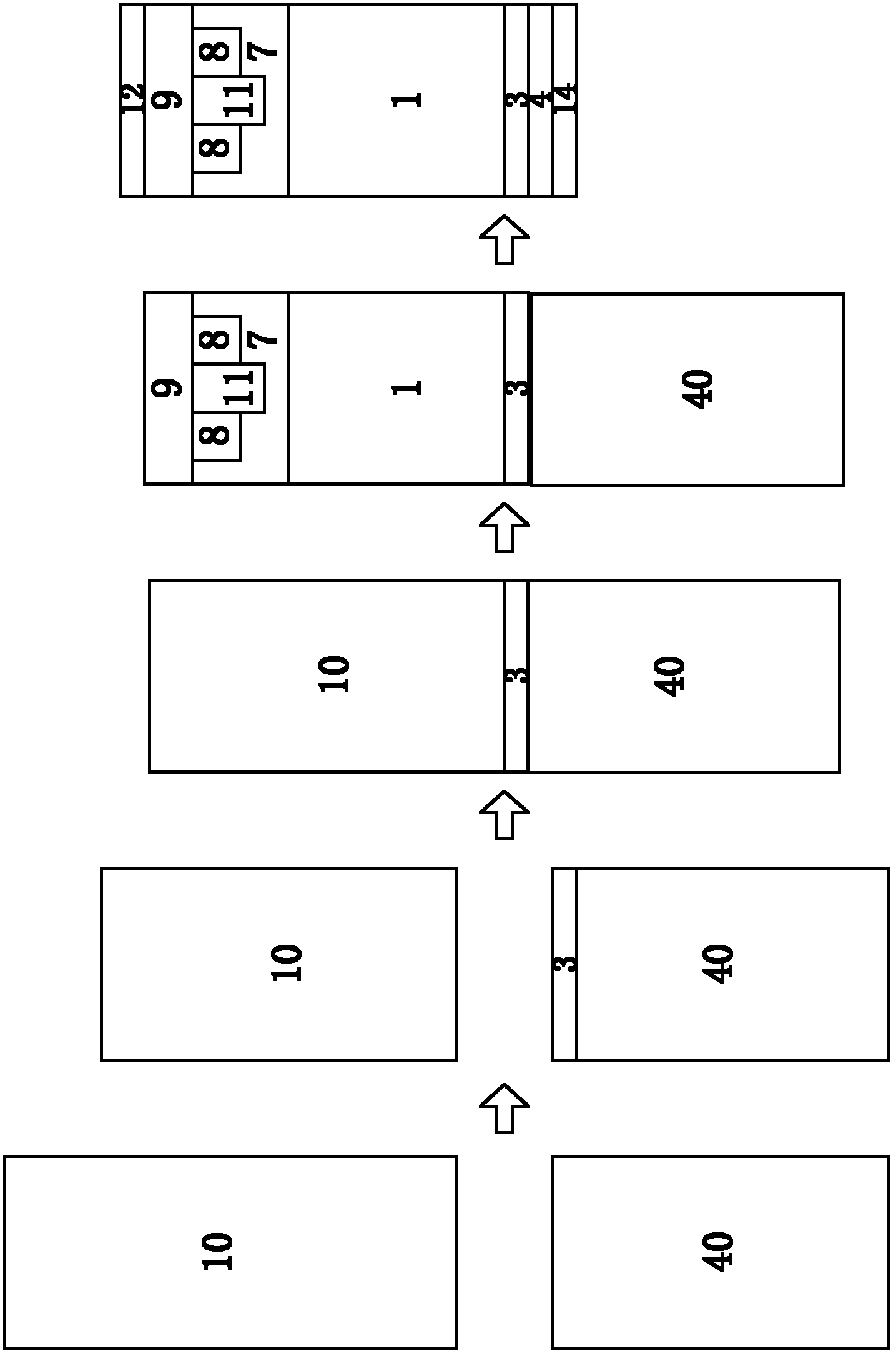
[0055] see Figure 4 , which is the second embodiment of the method for manufacturing a field-stop type IGBT device in the patch mode of the present invention, including the following steps:

[0056] In step 1', the first silicon substrate 10 and the second silicon substrate 40 of single-crystal silicon are selectively melted, and the first silicon substrate 10 is thinned to 50-300 μm, preferably 60 μm, and the second silicon substrate The front side of 40 forms n-type heavily doped field stop region 3 by ion implantation and annealing process.

[0057] In step 2', the second silicon substrate 40 is thinned from the back to 300-700 μm, preferably 600 μm.

[0058] In step 3', the back side of the first silicon substrate 10 and the front side of the second silicon substrate 40 (i.e. the surface of the n-type heavily doped field stop region 3) are formed into one body by a bonding process.

[0059] In the 4th step, the front structure of the IGBT device is manufactured on the f...


PUM


Abstract

The invention discloses a method of manufacturing a field termination type insulated gate bipolar translator (IGBT) component in a patching mode. The method comprises the steps of selecting a first silicon base and a second silicon base of floating zone single crystal silicon, thinning the thickness of the first silicon base, and forming an n-shaped heavy doping field blocking-up zone on the front surface of the second silicon base through ion injection and annealing technology; integrating the back face of the first silicon base and the front face of the second silicon base through bonding technology; manufacturing a front face structure of the IGBT component on the front face of the first silicon base until depositing front face metal as an emission electrode; and thinning the second silicon base from the back face, and depositing the back face metal as a collector. The method of manufacturing the IGBT component in the patching mode does not need production technology for extremely thin slices with thickness less than 70 nanometers, thereby effectively reducing the slice breaking rate of slice technology, and saving enormous cost of purchasing new machines and equipment.

Description

technical field [0001] The invention relates to a method for manufacturing an IGBT (Insulated Gate Bipolar Transistor, insulated gate bipolar transistor) device. Background technique [0002] The IGBT device is composed of a MOS transistor and a PNP bipolar transistor, and can also be regarded as composed of a VDMOS (Vertical double diffused MOSFET, vertical double diffused MOS transistor) and a diode. [0003] see figure 1 , which is a structural schematic diagram of a field stop (Field stop) IGBT device. On the back of the silicon wafer is a metal layer 14 as a collector, above which there is a p-type heavily doped collector region 4, further upward is an n-type heavily doped field blocking region 3, and further upward is an n-type medium and low doped region 1. There is a p well 7 in the n-type medium and low doping region 1 . The p well 7 has an n-type heavily doped source region 8 and a p-type heavily doped contact region 11 . There is a gate oxide layer 5 , an int...

Claims


Application Information

Patent Timeline
IPC IPC(8): H01L21/331
Inventor 颜树范张朝阳李江华房宝青华光平
Owner SHANGHAI HUAHONG GRACE SEMICON MFG CORP
Why Eureka
Try Eureka