Silicon through-hole test structure and corresponding test method

A technology of test structure and test method, applied in semiconductor/solid-state device test/measurement, measurement device, electromagnetic measurement device, etc., can solve the problems of high test cost, complex test structure, cumbersome detection, etc., and achieve simple structure and simple test. handy effect

Active Publication Date: 2013-06-05
SEMICON MFG INT (SHANGHAI) CORP
View PDF4 Cites 22 Cited by
  • Summary
  • Abstract
  • Description
  • Claims
  • Application Information

AI Technical Summary

Problems solved by technology

The U.S. patent document with the publication number US 2010 / 0313652 A1 discloses a method for measuring the depth of TSVs, but the method needs to form a microfluidic pressure sensing device on the surface of TSVs for detection, and the test structure is relatively complicated. Complicated and expensive to test

Method used


Image

  • Silicon through-hole test structure and corresponding test method
  • Silicon through-hole test structure and corresponding test method
  • Silicon through-hole test structure and corresponding test method

Examples


Embodiment Construction

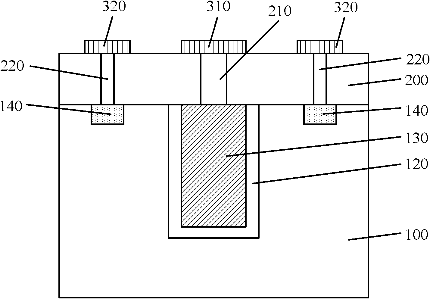
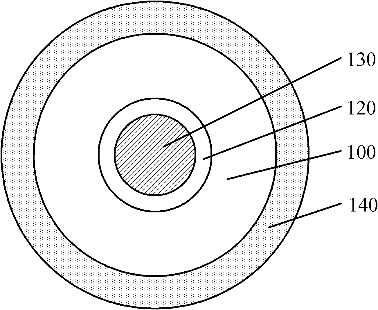
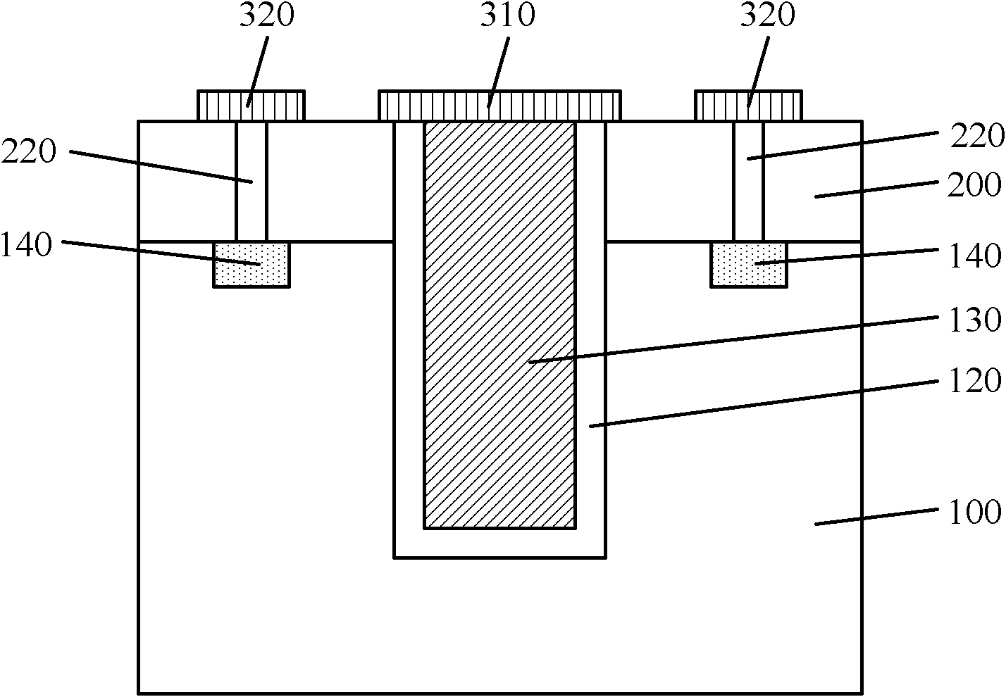
[0037] Since the depth of TSVs usually ranges from hundreds of nanometers to thousands of nanometers, and the diameter of TSVs is very small, it is difficult to etch silicon vias using conventional etching endpoint detection systems. The depth of the through-hole is precisely controlled, and if it is only controlled by the etching time, it is likely that the depth of the final formed through-silicon hole is very different from the standard value due to the difference in the wafer and the slight difference in the etching gas and power. . When the semiconductor substrate undergoes chemical mechanical polishing to expose the bottom of the through-silicon hole in the subsequent process, the through-silicon hole whose depth is greatly different from the standard value may not be exposed, making the electrical connection between different chips invalid. Therefore, in the existing technology, after the etching of the TSV is completed, the depth of the TSV needs to be detected, and un...


PUM


Abstract

The invention discloses a silicon through-hole test structure which comprises a semi-conductor substrate, a silicon through hole, insulation layers, conducting materials, a heavily doped area, a dielectric layer and metal interconnection layers, wherein the silicon through hole is located inside the semi-conductor substrate, the insulation layers are located on the side wall and the bottom surface of the silicon through hole, the conducting materials are filled into the silicon through hole and located on the surfaces of the insulation layers, the heavily doped area is arranged to surround the silicon through hole and located inside the semi-conductor substrate, the dielectric layer is located on the surface of the semi-conductor substrate, and the metal interconnection layers are located on the surface of the dielectric layer. The conducting materials in the silicon through hole is in electricity connection with a first metal interconnection layer, and the heavily doped area is in electricity connection with a second metal interconnection layer, and the conducting materials in the silicon through hole is in electricity isolation with the heavily doped area. When polarization voltages are applied across the conducting materials of the silicon through hole and the heavily doped area, and then whether the insulation layers are judged complete or not through that whether leakage currents are measured between the conducting materials and the heavily doped area or not, and the depth of the silicon through hole is judged to reach a standard value or not through a measured capacitance value between the conducting materials and the heavily doped area, and the test process is simple and convenient.

Description

technical field [0001] The invention relates to semiconductor testing technology, in particular to a through-silicon via testing structure and a corresponding testing method. Background technique [0002] With the continuous development of semiconductor technology, the feature size of semiconductor devices has become very small. It is becoming more and more difficult to increase the number of semiconductor devices in a two-dimensional packaging structure. Therefore, three-dimensional packaging has become a method that can effectively improve chip integration. degree method. Current three-dimensional packaging includes die stacking based on gold wire bonding, package stacking and three-dimensional stacking based on through silicon vias (Through Silicon Via, TSV). Among them, the three-dimensional stacking technology using through-silicon vias has the following three advantages: (1) high-density integration; (2) greatly shortening the length of electrical interconnections, so...

Claims


Application Information

Patent Timeline
Patent Type & Authority Applications(China)
IPC IPC(8): H01L21/66H01L23/544G01B7/26G01N27/00
Inventor 甘正浩三重野文健冯军宏
Owner SEMICON MFG INT (SHANGHAI) CORP
Why Eureka
Try Eureka