Photovoltaic device in double-absorption-layer PIN structure and manufacture method thereof

A double-absorbing layer, photovoltaic device technology, applied in photovoltaic power generation, semiconductor devices, electrical components, etc., can solve the problem of low utilization of sunlight

Inactive Publication Date: 2013-06-05
山东梁山義企重工机械股份有限公司
View PDF2 Cites 7 Cited by
  • Summary
  • Abstract
  • Description
  • Claims
  • Application Information

AI Technical Summary

Problems solved by technology

[0005] The purpose of the present invention is to solve the problem that the traditional wide-bandgap oxide thin film solar cells do not have a high utilization rate of sunlight, and propose a double-absorbing layer PIN structure photovoltaic device and its preparation method to more effectively utilize sunlight and improve conversion efficiency

Method used


Image

  • Photovoltaic device in double-absorption-layer PIN structure and manufacture method thereof
  • Photovoltaic device in double-absorption-layer PIN structure and manufacture method thereof
  • Photovoltaic device in double-absorption-layer PIN structure and manufacture method thereof

Examples


Embodiment 1

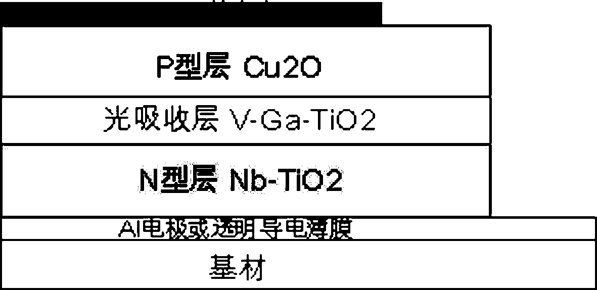
[0018] with attached figure 1 The device structure shown, select Nb:TiO 2 Doping concentration 1.7×10 21 cm -3 , thickness 10nm, intermediate layer (V-Ga:TiO 2 layer) with a doping concentration of 10 16 cm -3 , with a thickness of 100nm, Cu 2 O doping concentration 10 18 cm -3 , thickness 300nm.

[0019] The battery efficiency under these parameters is simulated to be 34.12%, and the fill factor is 0.83.

Embodiment 2

[0021] with attached figure 1 The device structure shown, select Nb:TiO 2 Doping concentration 1.7×10 21 cm -3 , thickness 10nm, intermediate layer (V-Ga:TiO 2 layer) with a doping concentration of 10 18 cm -3 , with a thickness of 100nm, Cu 2 O doping concentration 10 18 cm -3 , thickness 300nm.

[0022] The battery efficiency under this parameter is simulated to be 34.121%, and the fill factor is 0.83.

Embodiment 3

[0024] Attached figure 1 The device structure shown, select Nb:TiO 2 Doping concentration 1.7×10 21 cm -3 , thickness 10nm, intermediate layer (V-Ga:TiO 2 layer) with a doping concentration of 10 12 cm -3 , with a thickness of 100nm, Cu 2 O doping concentration 10 18 cm -3 , thickness 300nm.

[0025] The battery efficiency under this parameter is simulated to be 34.136%, and the fill factor is 0.831.

[0026] All simulations use the standard solar spectrum of AM1.5 as the light source.


PUM

PropertyMeasurementUnit
thicknessaaaaaaaaaa
thicknessaaaaaaaaaa
thicknessaaaaaaaaaa

Abstract

The invention discloses a photovoltaic device in a double-absorption-layer PIN structure and a manufacture method thereof. Two types of materials of V and Ga with different band gap widths are added into heterojunction, TiO2(1.6eV) and Cu2O(2.0eV) serve as a light double-absorption layer, an absorbing band for generating a photon-generated carrier is expanded, and a principle limit of a single-stage cell is broken. The structure of the photovoltaic device is that a metal and a transparent conducting thin film serve as a bottom electrode of the device, niobium mixed with titanium dioxide serves as an N-type layer of the device, vanadium and gallium jointly mixed with the titanium dioxide are arranged on the N-type layer to serve as a light absorbing layer of the device, the Cu2O serves as a P-type layer of the device and also an absorption layer of the device, and metals of Pt and the like serve as anode of the cell. According to the photovoltaic device in double-absorption-layer PIN structure and the manufacture method of the photovoltaic device, an N-type heavy mixing layer Nb of TiO2 is design, height of a self-established electric field is increased, open-circuit voltage is increased, and theoretical conversion efficiency of device performance is as high as 34%. The design of the three-layer PIN structure comprising the double absorption layers enables light absorption range to cover visible light and a near infrared area, sunlight is effectively absorbed, and conversion efficiency of a thin-film solar cell is greatly improved.

Description

technical field [0001] The invention relates to the field of thin-film solar cells, in particular to a double-absorbing layer PIN structure photovoltaic device and a preparation method. Background technique [0002] The energy problem is a serious challenge to realize the sustainable development of economy and society. Solar radiation is the Earth's largest source of clean, green energy. Photovoltaic power generation is one of the first choices for human beings to solve energy problems. [0003] At present, mature or nearly mature photovoltaic cells on the market include crystalline silicon cells, amorphous silicon thin-film cells, compound thin-film cells such as CuInGaSe or CdS / CdTe, dye-sensitized cells, and organic-inorganic composite cells. However, these batteries still have some unresolved issues in terms of cost, stability, limitations of production raw materials, or environmental protection of the production process. The all-oxide solar cell is a new concept prop...

Claims


Application Information

Patent Timeline
Patent Type & Authority Applications(China)
IPC IPC(8): H01L31/075H01L31/0352H01L31/18
CPCY02E10/50Y02E10/548Y02P70/50
Inventor 高云郭美澜肖永跃夏晓红黄忠兵邵国胜
Owner 山东梁山義企重工机械股份有限公司
Why Eureka
Try Eureka