Super-diffraction nano-optical probe

A nano-optics and super-diffraction technology, applied in the field of bow-tie structure, can solve the problems that restrict the photolithographic resolution of SNOM probes, and achieve the effect of simple structure and cheap materials

Inactive Publication Date: 2013-06-12
INST OF OPTICS & ELECTRONICS - CHINESE ACAD OF SCI
View PDF4 Cites 18 Cited by
  • Summary
  • Abstract
  • Description
  • Claims
  • Application Information

AI Technical Summary

Problems solved by technology

This contradiction greatly restricts t

Method used


Image

  • Super-diffraction nano-optical probe
  • Super-diffraction nano-optical probe
  • Super-diffraction nano-optical probe

Examples


Embodiment Construction

[0010] The present invention will be described in detail below in conjunction with the accompanying drawings and specific embodiments, but the scope of protection of the present invention is not limited to the following examples, but should include all content in the claims.

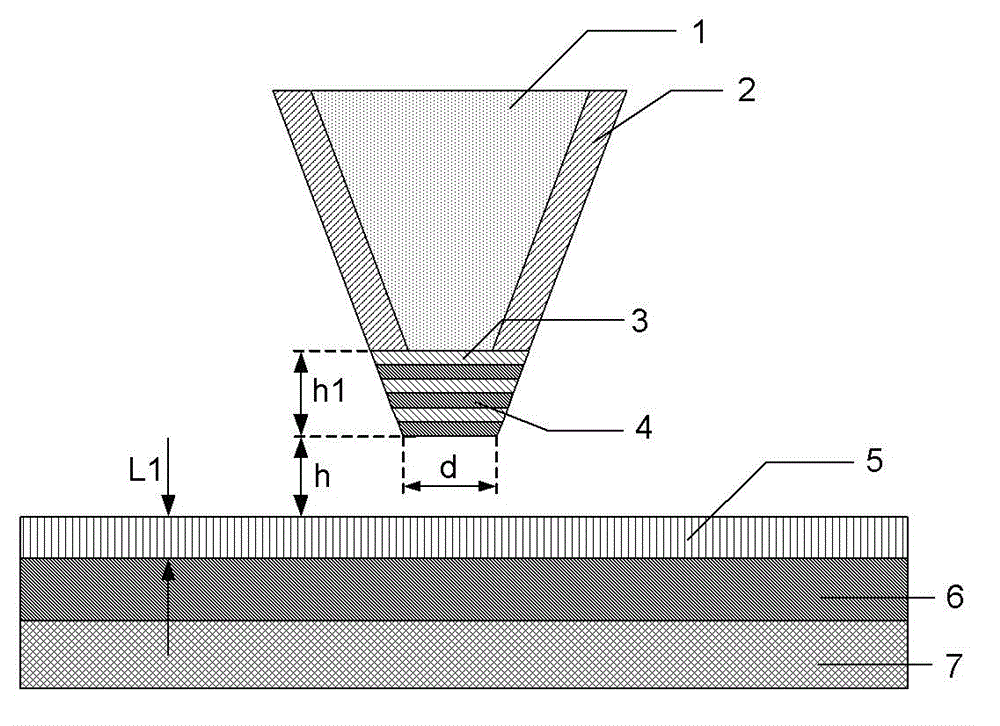
[0011] see figure 1 , is a cross-sectional view of the structure of the superdiffraction nano-optical probe included in the present invention, the optical probe includes a tapered dielectric core 1, a metal outer cladding 2, a dielectric film 3 and a metal film layer 4, and the tapered dielectric core 1 The top is a platform-shaped tapered tip; a layer of metal outer cladding 2 is coated on the outer surface of the tapered dielectric core 1, and a multilayer film is deposited on the surface of the tapered needle tip. The multilayer film is composed of alternately arranged dielectric films 3 and the metal film layer 4, when the light is vertically incident on the surface of the dielectric film 3, surface ...


PUM

PropertyMeasurementUnit
Diameteraaaaaaaaaa

Abstract

The invention relates to a super-diffraction nano-optical probe. Specifically, a metal outer cladding is plated on the outer surface of conical medium core, and a multilayer film is deposited on the surface of a conical needle tip. The multilayer film is composed of dielectric films and metal film layers that are arranged alternately. Vertically incident light on the surfaces of the dielectric films can excite surface plasmon polaritons on interfaces of the metal films and the dielectric films. When the urface plasmon polaritons spread to the conical needle tip along the interfaces, a local enhancement effect can be achieved, and further, modification, compression and transmission enhancement on local enhanced light spots can be carried out through optical anisotropy of the multilayer film on the surface of the conical needle tip. According to the same principle, the invention also includes a design of a bow-tie structure with the multilayer film material deposited on its surface. The bow-tie structure is characterized in that the multilayer film material is deposited on its lower surface. According to the invention, the transmitted light intensity can also be changed by adjusting the thickness ratio of metal media in the multilayer film. Also, the probe has a simple structure, and can be applied to lithography very conveniently to improve lithographic resolution.

Description

technical field [0001] The invention relates to photolithographic direct writing technology, in particular to a superdiffraction nanometer optical probe and a bowtie structure with multi-layer film materials deposited on the surface. Background technique [0002] In recent years, nanolithography technology has been developed by leaps and bounds. Plasma direct writing nanolithography (plasmonic direct writing nanolithography) technology has the advantages of short production cycle and flexible writing structure compared with traditional masked lithography; compared with expensive electron beam lithography, As far as focused ion beam lithography is concerned, the cost has been greatly reduced, making it more and more widely used, and gradually becoming the most potential lithography technology. The most important one in plasma direct writing nanolithography technology is the near-field optical microscope (SNOM) probe-based lithography technology, in which the probe is the mos...

Claims


Application Information

Patent Timeline
IPC IPC(8): G03F7/20G01Q60/22G02B27/58
Inventor 罗先刚赵泽宇王长涛王彦钦陶兴胡承刚高平黄成姚纳罗云飞
Owner INST OF OPTICS & ELECTRONICS - CHINESE ACAD OF SCI
Why Eureka
Try Eureka