Gallium nitride base light-emitting diode with composite potential barrier

A technology of light-emitting diodes and recombination barriers, applied in electrical components, circuits, semiconductor devices, etc., can solve problems such as lattice mismatch, achieve uniform distribution, improve recombination efficiency, and improve performance

Active Publication Date: 2013-06-12
SOUTHEAST UNIV
View PDF12 Cites 19 Cited by
  • Summary
  • Abstract
  • Description
  • Claims
  • Application Information

AI Technical Summary

Problems solved by technology

[0029] Although the use of AlInGaN can reduce the polarization effect, thereby reducing the built-in electric field caused by the polarization effect, when using AlInGaN to replace the traditional GaN barrier, the composition of Al and In is In in the InGaN potential well layer Calculated with a given composition, so it is still possible to retain a certain lattice mismatch between AlInGaN and InGaN

Method used


Image

  • Gallium nitride base light-emitting diode with composite potential barrier
  • Gallium nitride base light-emitting diode with composite potential barrier
  • Gallium nitride base light-emitting diode with composite potential barrier

Examples


Embodiment 1

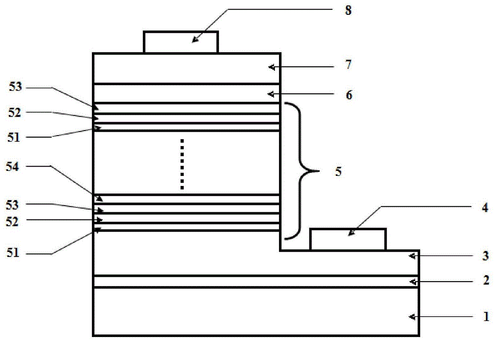
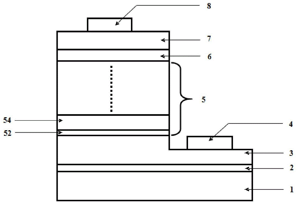
[0058] Assuming the following GaN-based LED In u Ga 1-u The In composition in the N well layer 51 is u=0.2.

[0059] figure 1 What is shown is the structural schematic diagram of the GaN-based LED with composite potential barrier according to the present invention. The structural elements of this LED include: sapphire substrate 1, buffer layer 2, n-type gallium nitride epitaxial layer 3, n-type electrode 4, multi-quantum well active region 5, indium gallium nitride potential well layer 51, the first AlGaInN layer 52 , GaN layer 53 , second AlGaInN layer 54 , p-type AlGaN epitaxial layer 6 , p-type GaN epitaxial layer 7 , and p-type electrode 8 .

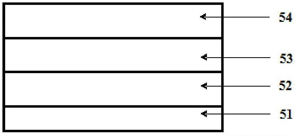
[0060] image 3 Shown is a schematic diagram of a single quantum well with a first-type composite barrier layer of AlInGaN-GaN-AlInGaN, including In 0.2 Ga 0.8 NInGaN potential well layer 51, the first AlGaInN layer 52, the first AlGaInN layer 52 and In 0.2 Ga 0.8 At the interface where the NInGaN layer 51 contacts, according...


PUM

PropertyMeasurementUnit
thicknessaaaaaaaaaa

Abstract

The invention discloses a gallium nitride base light-emitting diode with a composite potential barrier. The gallium nitride base light-emitting diode comprises a sapphire substrate, a buffering layer, an n-type gallium nitride epitaxial layer, a multiple quantum well active area, a p-type algan epitaxial layer and a p-type gallium nitride epitaxial layer, wherein the sapphire substrate, the buffering layer, the n-type gallium nitride epitaxial layer, the multiple quantum well active area, the p-type algan epitaxial layer and the p-type gallium nitride epitaxial layer are arranged sequentially from bottom to top. A p-type metal electrode is arranged on the upper surface of the p-type gallium nitride epitaxial layer. An n-type electrode is arranged on a lower platform surface of the n-type gallium nitride epitaxial layer. The multiple quantum well active area comprises 5-20 indium gallium nitride potential well layers which are arranged at intervals from bottom to top. A first kind composite potential barrier layer is arranged between every two indium gallium nitride potential barrier layers. A second kind composite potential well layer is arranged on the upper surface of an indium gallium nitride potential well layer at the top layer. According to the composite potential barrier, at the contact position of an aluminum, gallium and indium nitride layer and an InGaN potential well layer, a built-in electric field which is produced due to a polarization effect can be decreased through adjustment of aluminum (Al) and indium (In). On a contact interface between an AlInGaN layer and a GaN layer, a ratio between the Al and the In is adjusted to be 0.83:0.17, and lattices of the Al and the In are enabled to be matched.

Description

technical field [0001] The invention belongs to the field of semiconductor lighting and relates to a gallium nitride-based LED with composite potential barriers. Background technique [0002] GaN-based LEDs have entered the market and made great progress, but the problem of low light emission efficiency of chips has not been well resolved. The reason is that there are polarization effects in III-V nitride light-emitting elements, including spontaneous polarization and piezoelectric polarization. Spontaneous polarization is caused by the asymmetry of the wurtzite structure in the [0001] direction, while piezoelectric polarization is caused by stress at the heterojunction interface due to lattice mismatch between different materials, making the anion The arrangement of cations and cations moves, resulting in the piezoelectric effect of polarized charges. The built-in polarization electric field caused by the polarization effect is a strong electric field, which causes seriou...

Claims


Application Information

Patent Timeline
Patent Type & Authority Applications(China)
IPC IPC(8): H01L33/06H01L33/32
Inventor 张雄许洁崔一平
Owner SOUTHEAST UNIV
Why Eureka
Try Eureka