

Device components with surface-embedded additives and related manufacturing methods
A technology of additives and embedding regions, applied in the direction of electrical components, semiconductor devices, circuit optical components, etc., can solve problems such as poor adhesion, non-uniform mixing and cohesion, and high layering
- Summary
- Abstract
- Description
- Claims
- Application Information
AI Technical Summary
Problems solved by technology
Method used
Image

Examples
example 1
[0228] Formation of surface-embedded encapsulation layer
[0229] This example illustrates the formation of a surface-embedded encapsulation layer with spectral shifting capabilities that can be laminated adjacent to the front surface of a solar device. Sheets of ethylene vinyl acetate (or EVA) can be sprayed with a solvent system and a solution of phosphor. Another encapsulation material, such as polyvinyl alcohol (or PVA), polyvinyl butyral (or PVB), or thermoplastic polyurethane (or TPU), can be used instead of, or in combination with, EVA. The EVA sheet may be between about 250 μm and about 2.5 mm thick, such as about 500 μm thick. As an example, the solvent system may be combined tetrahydrofuran and dichloromethane, and the phosphor may be a downshifting species such as tris(dibenzoylmethane)(o-phenanthroline)europium(III) (or Eu( dbm) 3 phen), and tris[3-(trifluoromethylhydroxymethylene)-d-camphorate]europium(III) (or Eu(tfc) 3 ) either or both. Another solvent or c...
example 2
[0231] Formation of surface-embedded encapsulation layer
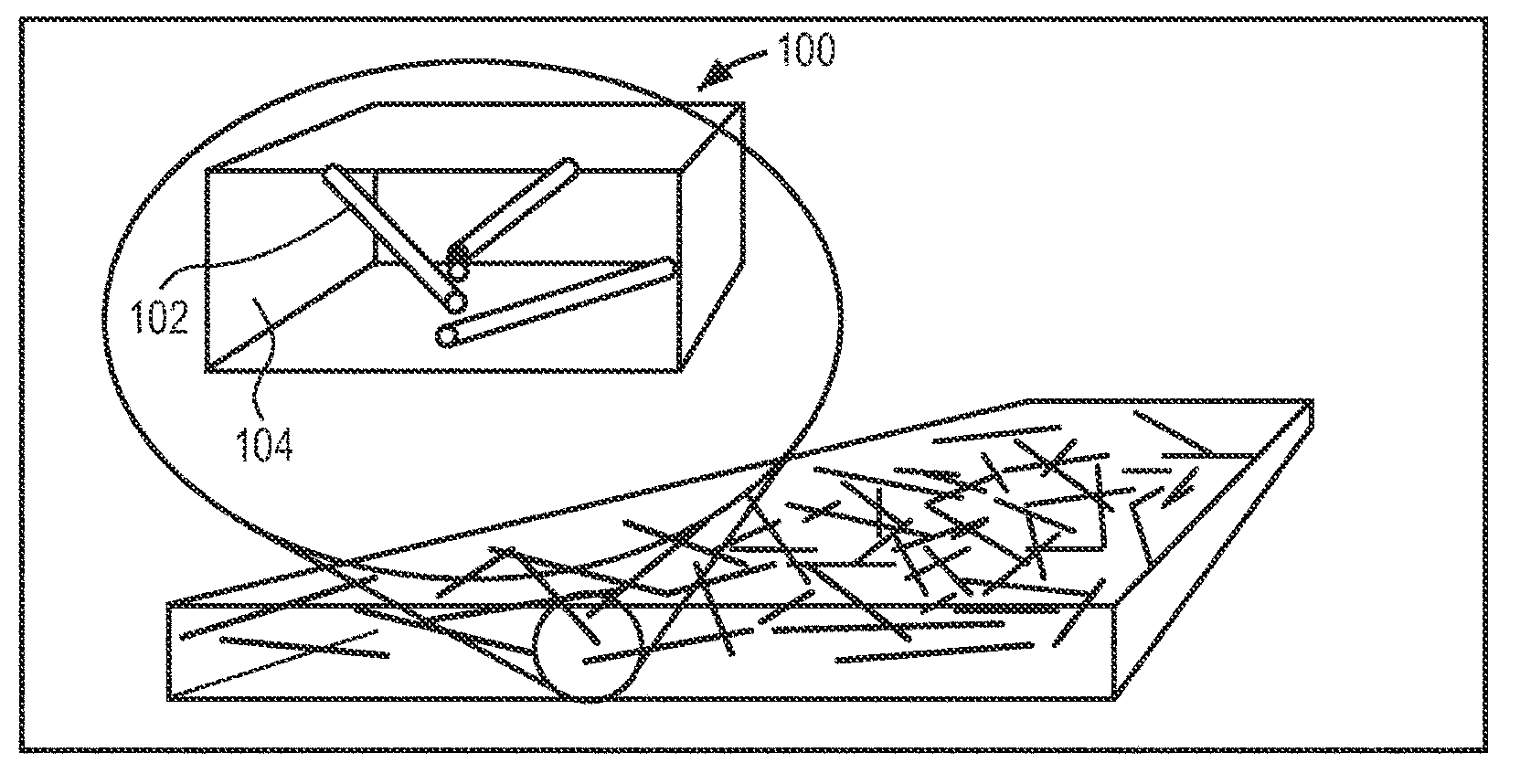
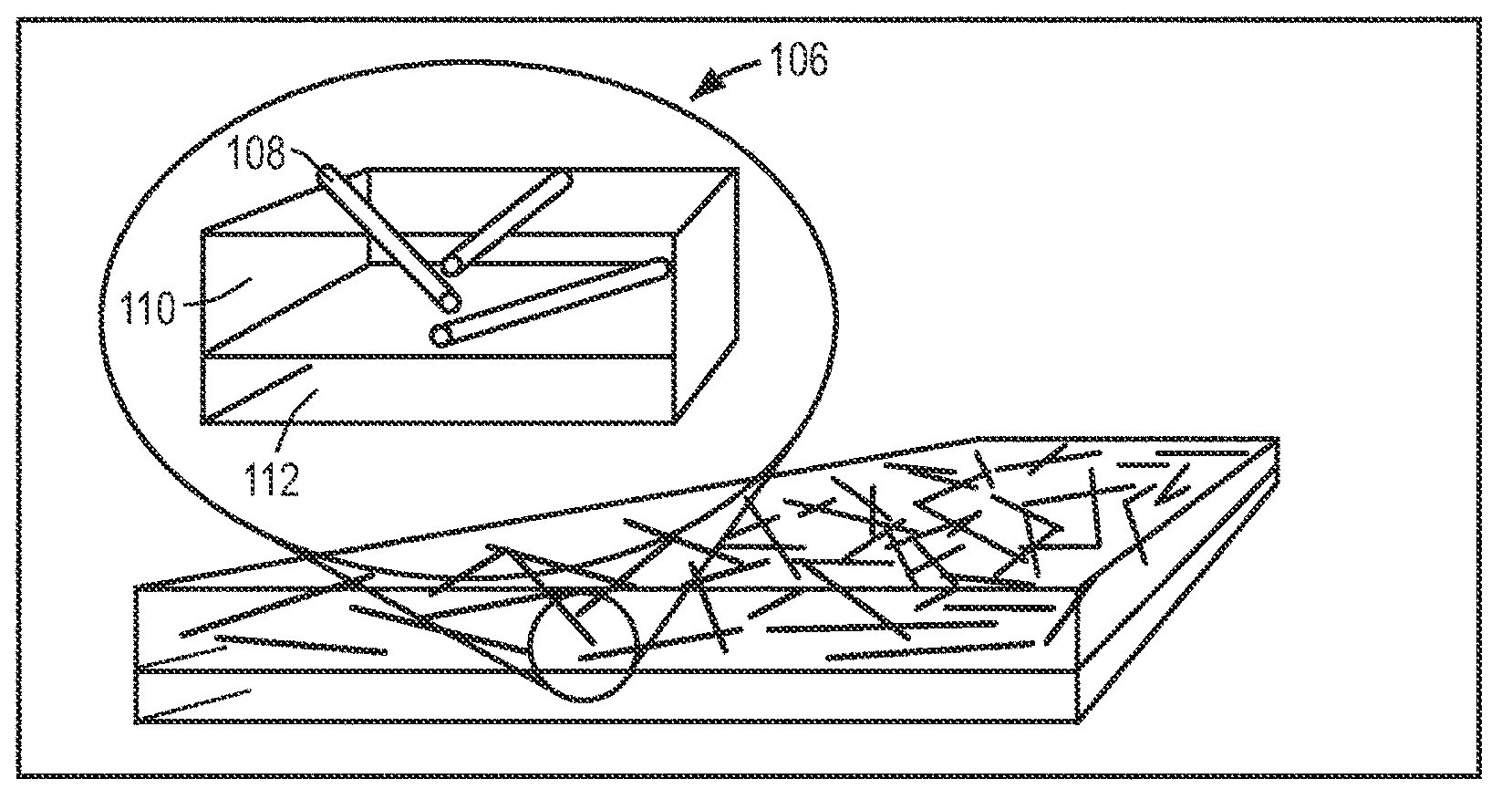
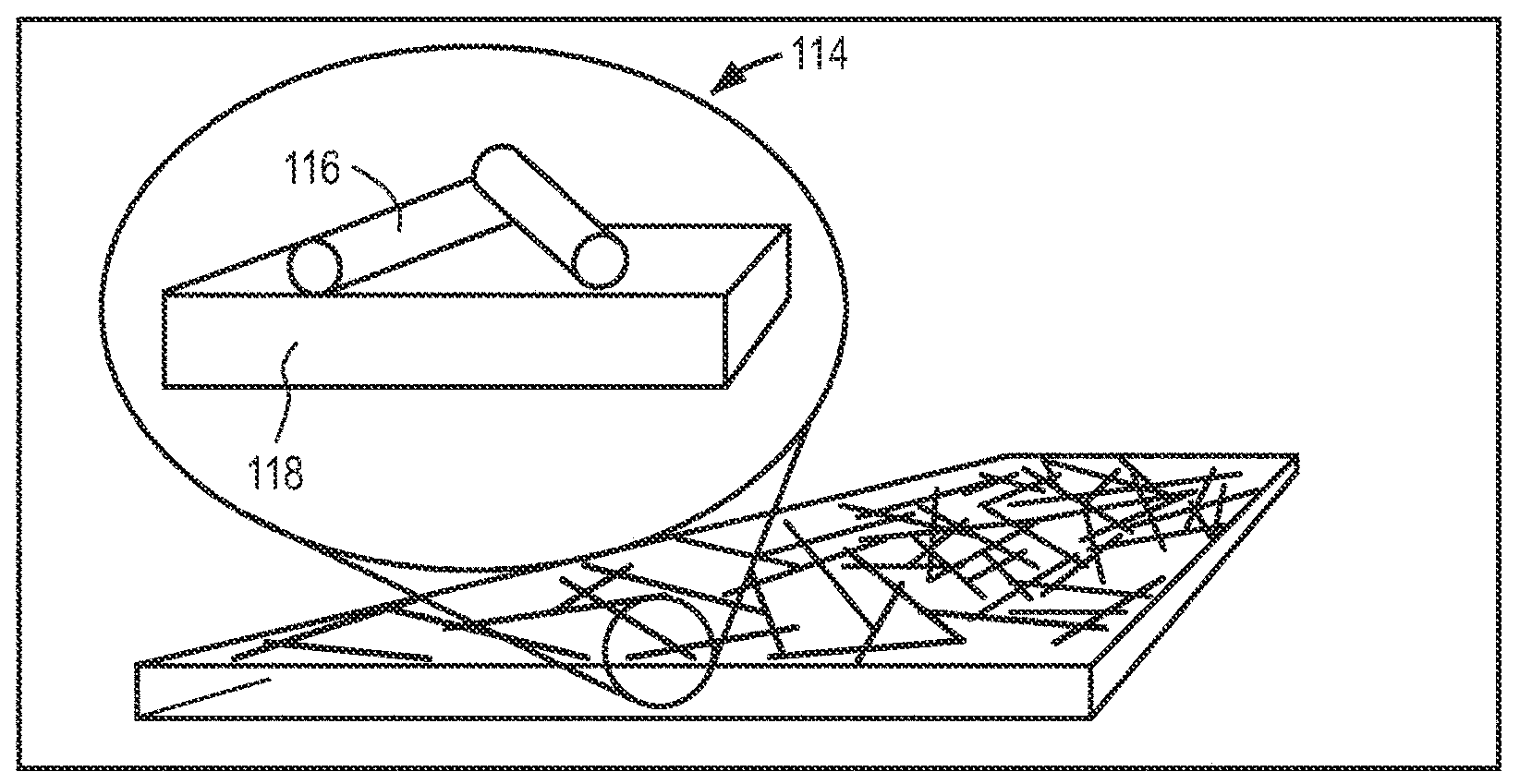
[0232] This example illustrates the formation of surface-embedded encapsulation layers that can be incorporated in solar devices. Additives suspended in alcohol, such as in the form of silver nanowires, are sprayed onto the surface of the EVA sheet. After the alcohol had evaporated leaving a surface deposited layer of silver nanowires on top of the EVA sheet, tetrahydrofuran was sprayed onto the surface of the EVA, softening and embedding the nanowires into the EVA sheet. The amount of tetrahydrofuran can be controlled to adjust the degree of intercalation of the nanowires partially or fully embedded under the surface of the EVA sheet. The resulting nanowire-embedded EVA sheet can exhibit light scattering properties and electrical conductivity due to the infiltration of contact nanowires adjacent to the surface of the EVA sheet. This embedding process can be performed under greenhouse and atmospheric pressure. The n...
example 3
[0234] Formation of surface-embedded encapsulation layer
[0235] About 250mg of Eu(dbm) 3 The phen is combined with about 13ml of tetrahydrofuran. The bulk of this solution was sprayed with an iwata Eclipse HP-CS brush on a 19 cm x 27 cm block of Mars Rock EVA sheet to provide approximately 0.487 mg / cm 2 cover. The EVA flakes were cut into 2.1 inch by 2.1 inch pieces. A 2 inch by 2 inch piece of borosilicate float glass from McMaster was cleaned with Micro90 cleaner and rinsed with deionized water and isopropanol, followed by approximately 30 minutes of UV-ozone treatment. Glass blocks are laminated into crystalline silicon photovoltaic cells obtained from MarsRock. One block is laminated with untreated EVA. Another block was laminated with EVA treated with europium phosphor. Lamination was performed by sandwiching each block of EVA between a block of glass and the photovoltaic cell, followed by the application of vacuum starting at about 99°C with a vacuum. The assemb...
PUM
| Property | Measurement | Unit |
|---|---|---|
| diameter | aaaaa | aaaaa |
| length | aaaaa | aaaaa |
| length | aaaaa | aaaaa |
Abstract
Description
Claims
Application Information