Novel silicon substrate low resistance inductance structure and wafer level encapsulating method thereof

A silicon wafer and silicon-based technology, applied in the field of new silicon-based low-resistance inductance structure and its wafer-level packaging, can solve the problems of limited packaging density, difficult process, easy to have residual glue, etc., to reduce DC resistance, The effect of reducing process difficulty and improving quality factor

Active Publication Date: 2013-06-19
JIANGYIN CHANGDIAN ADVANCED PACKAGING CO LTD
View PDF6 Cites 12 Cited by
  • Summary
  • Abstract
  • Description
  • Claims
  • Application Information

AI Technical Summary

Problems solved by technology

The following process problems exist in the thick resist process: after the photoresist is spin-coated, the uniformity of the resist thickness is poor; the photolithography exposure process is difficult to control due to the uneven thickness of the photoresist; Residue
Therefore, using the above process, that is, the rewiring method in which the photoresist forms the wiring pattern, and the wiring layer is arranged on the surface of the silicon base body, the requirements for the photoresist material are high, the process is difficult, the process cost is high, and the packaging density is also limited. promotion

Method used


Image

  • Novel silicon substrate low resistance inductance structure and wafer level encapsulating method thereof
  • Novel silicon substrate low resistance inductance structure and wafer level encapsulating method thereof
  • Novel silicon substrate low resistance inductance structure and wafer level encapsulating method thereof

Examples


Embodiment Construction

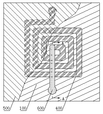
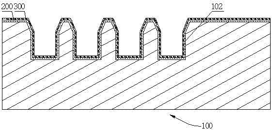
[0050] see figure 1 and figure 2 , the present invention is a novel silicon-based low-resistance inductance structure, including a silicon base body 101, on which a concave coil slot 102 is arranged, and the coil slot 102 can be distributed in a spiral shape. The inclination angle of the side wall of the coil slot 102 is α, the inclination angle of the upper edge of the side wall is β, and α≧β. Preferably, the value range of the inclination angle α of the side wall of the coil slot 102 is: 80°≦α≦90°, and the value range of the inclination angle β along the side wall is: 50°≦α≦70°.

[0051] The bottom and side walls of the coil slot 102 and the upper surface of the silicon base body 101 are coated with an insulating layer 200 of organic material. A single-layer metal or multi-layer electroplating seed layer 300 is disposed on the insulating layer 200 inside the coil slot 102 . A metal wiring layer 400 is provided in the coil slot 102 where the electroplating seed layer 300...


PUM


Abstract

The invention relates to a novel silicon substrate low resistance inductance structure and a wafer level encapsulating method of the novel silicon substrate low resistance inductance structure, and belongs to the technical field of semiconductor encapsulation. A coil groove (102) is formed in the upper surface of a silicon wafer (100) in an etching mode, an insulation layer (300) is coated inside the coil groove (102), an electroplating seed layer (300) is arranged in a deposit mode through a physical method, a thick copper metal wiring layer (400), namely an inductance coil, is formed in the coil groove (102) in a photoetching imaging mode through an electroplating technology, and finally, a secondary passivating layer (500) and metal leading wires (600) are arranged on the thick copper metal wiring layer (400), and the thick copper metal wiring layer (400) is communicated with the thick copper metal wiring layer (400) through an secondary passivating layer opening (501). According to the novel silicon substrate low resistance inductance structure and a wafer level encapsulating method of the novel silicon substrate low resistance inductance structure, the copper metal wiring layer serving as the inductance coil is embedded into the interior of a silicon substrate body, technological difficulty and technological cost of preparation of the inductance coil are reduced, an encapsulating density is improved, meanwhile direct current resistance of an inductor is reduced by increasing the thickness of coils, and a quality factor of the inductor is improved.

Description

technical field [0001] The invention relates to a novel silicon-based low-resistance inductance structure and a wafer-level packaging method thereof, belonging to the technical field of semiconductor packaging. Background technique [0002] With the development of packaging technology, system-in-package (SIP, system in package) is becoming more and more popular due to its better electrical performance and smaller package size. In the packaging field of power management devices such as DC-DC converters, people try to integrate discrete inductors and power management chips into a system-in-package, but the current ceramic-based discrete inductors are large in size and cannot meet the requirements of miniaturization of the package. Silicon-based planar spiral inductors are an alternative to discrete inductors due to their small size and high precision. [0003] At present, the wiring process on the silicon substrate used to make silicon-based spiral inductors is mainly a rewir...

Claims


Application Information

Patent Timeline
Patent Type & Authority Applications(China)
IPC IPC(8): H01L23/522H01L21/768
Inventor 郭洪岩张黎陈锦辉赖志明
Owner JIANGYIN CHANGDIAN ADVANCED PACKAGING CO LTD
Why Eureka
Try Eureka