Thin film transistor array substrate, method for manufacturing the same, and annealing oven for performing the same method

A technology for thin film transistors and array substrates, applied in the field of thin film transistor array substrates, can solve problems such as burning, inability of an organic protective layer to withstand high temperatures, and oxidation phenomena.

Active Publication Date: 2015-07-15
E INK HLDG INC
View PDF2 Cites 0 Cited by
  • Summary
  • Abstract
  • Description
  • Claims
  • Application Information

AI Technical Summary

Problems solved by technology

[0004] However, if an organic protective layer is used as a passivation layer, the annealing process in an oxygen-containing environment will cause the oxidation of the drain / source metal at the same time because the organic protective layer cannot withstand high temperatures, resulting in an increase in the resistance of the wire, or even The problem of uneven line impedance
[0005] In addition, high concentration of oxygen is used as the reaction gas required for the annealing process. Due to the use of high oxygen concentration at high temperature, it may cause severe oxidation phenomena, such as combustion or even explosion.

Method used


Image

  • Thin film transistor array substrate, method for manufacturing the same, and annealing oven for performing the same method
  • Thin film transistor array substrate, method for manufacturing the same, and annealing oven for performing the same method
  • Thin film transistor array substrate, method for manufacturing the same, and annealing oven for performing the same method

Examples


Embodiment Construction

[0047] The following will clearly illustrate the spirit of the present invention with the accompanying drawings and detailed descriptions. After those skilled in the art understand the embodiments of the present invention, they can be changed and modified by the techniques taught in the present invention without departing from the present invention. spirit and scope.

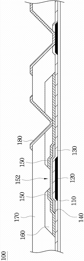
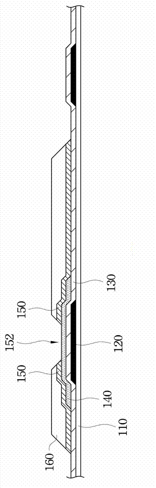
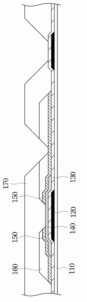
[0048] see figure 1 , which shows a schematic cross-sectional view of the thin film transistor array substrate 100 according to an embodiment of the present invention. Such as figure 1 As shown, the thin film transistor array substrate 100 includes a substrate 110, a gate layer 120, an insulating layer 130, an oxide semiconductor layer 140, a source / drain layer 150, an organic acrylic photoresist 160, a protective layer 170 and a conductive layer. 180.

[0049] The gate layer 120 is formed on the substrate 110 . In this embodiment, the substrate 110 may be a resin substrate, an organic polymer substrate or a...


PUM


Abstract

A thin film transistor (TFT) array substrate includes a substrate, a gate electrode layer disposed on the substrate, an insulating layer, an oxide semiconductor layer disposed on the insulating layer, a source / drain electrode layer, an organic-acrylic photoresist layer, a passivation layer and an electrically conductive layer. The insulating layer is disposed on the gate electrode layer and the substrate. The source / drain electrode layer is disposed on the insulating layer and the oxide semiconductor layer, and a gap is formed through the source / drain electrode layer for exposing the oxide semiconductor layer therethrough. The organic-acrylic photoresist layer covers the source / drain electrode layer. The passivation layer is disposed on the substrate, the oxide semiconductor layer and the organic-acrylic photoresist layer. The electrically conductive layer is disposed on the passivation layer or the organic-acrylic photoresist layer and connected to the source / drain electrode layer or the gate electrode layer.

Description

technical field [0001] The invention relates to a thin film transistor array substrate, in particular to a thin film transistor array substrate of a display. Background technique [0002] In recent years, a thin film transistor (Film Transistor, TFT) using a transparent amorphous oxide semiconductor film containing indium, gallium, zinc, and oxygen as a channel layer has been actively developed. [0003] In the semiconductor manufacturing process, when the semiconductor is doped with impurities such as boron, phosphorus or arsenic, a large number of vacancies will be generated, which will cause the arrangement of atoms to be disordered, resulting in drastic changes in the properties of the semiconductor material. Therefore, annealing is required to restore the crystal structure and eliminate defects. The impurity atoms at the formula positions are brought into replacement positions by annealing. The annealing process in an oxygen-containing environment is already a necessar...

Claims


Application Information

Patent Timeline
Patent Type & Authority Patents(China)
IPC IPC(8): H01L27/02H01L29/786H01L21/77H01L21/67
CPCH01L27/1248H01L27/1225H01L29/78606
Inventor 蓝纬洲辛哲宏吴幸怡
Owner E INK HLDG INC
Why Eureka
Try Eureka