Multimode wide-band filter based on multi-branch loaded square resonance ring

A resonant ring and filter technology, which is applied in the direction of resonators, waveguide devices, electrical components, etc., can solve the problems of limiting the size of the filter circuit and failing to meet the needs of miniaturization of the filter, and achieve the reduction of standing waves and size reduction , Improve the effect of out-of-band suppression

Active Publication Date: 2013-07-03
XIDIAN UNIV
View PDF8 Cites 14 Cited by
  • Summary
  • Abstract
  • Description
  • Claims
  • Application Information

AI Technical Summary

Problems solved by technology

However, the traditional multimode wideband filter is based on a closed loop, and its center frequency basically resonates at the resonant frequency of the closed loop. The perimeter of the closed loop limits the circuit size of the filter, which cannot meet the needs of modern communication systems. The need for filter miniaturization

Method used


Image

  • Multimode wide-band filter based on multi-branch loaded square resonance ring
  • Multimode wide-band filter based on multi-branch loaded square resonance ring
  • Multimode wide-band filter based on multi-branch loaded square resonance ring

Examples


Embodiment 1

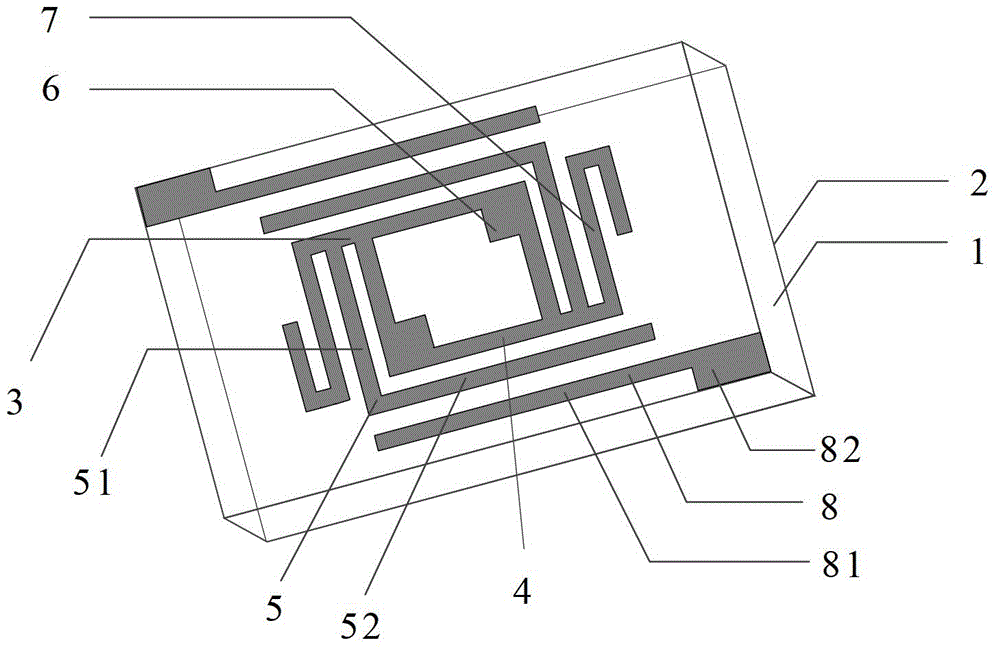
[0035] refer to figure 1 and figure 2 , the present invention includes a microstrip dielectric substrate 1, a metal ground plate 2, a square resonant ring 3 and a pair of input and output feeders 8; the square resonant ring 3 includes a square metal ring 4, a pair of equal-length perturbation branches 5, A pair of identical impedance-matching metal sheets 6 and a pair of equal-length folded transmission zero-point stubs 7 . in:

[0036] The microstrip dielectric substrate 1 adopts a single-sided copper-clad dielectric substrate with a dielectric constant of 2.65 and a thickness of 1 mm;

[0037] The lower layer of the microstrip dielectric substrate 1 is a copper-clad grounding plate 2, the square resonant ring 3 is located on the upper layer of the microstrip dielectric substrate 1, and the perimeter of the square metal ring 4 satisfies: Among them, L 1 and L 2 is the length of the two sides of the square metal ring 4 and satisfies: L 2 ≤ L 1 ≤2L 2 ,λ g is the wave...

Embodiment 2

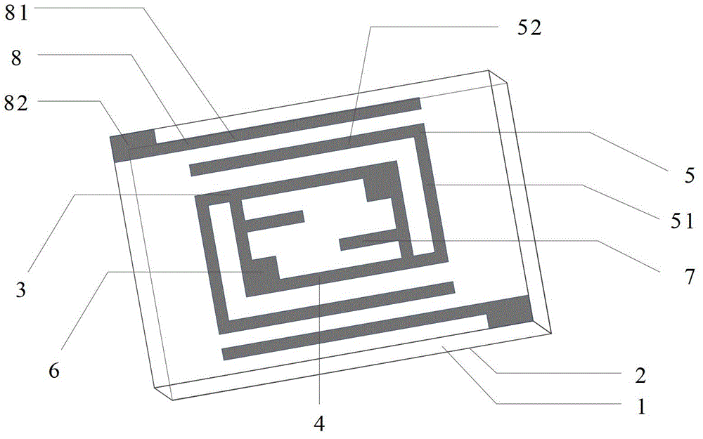
[0050] refer to image 3 and Figure 4 , the present invention includes a microstrip dielectric substrate 1, a metal ground plate 2, a square resonant ring 3 and a pair of input and output feeders 8; the square resonant ring 3 includes a square metal ring 4, a pair of equal-length perturbation branches 5, A pair of identical impedance-matching metal sheets 6 and a pair of transmission zero stubs 7 of equal length. in:

[0051] The microstrip dielectric substrate 1 adopts a single-sided copper-clad dielectric substrate with a dielectric constant of 2.65 and a thickness of 1 mm;

[0052] The lower layer of the microstrip dielectric substrate 1 is a copper-clad grounding plate 2, the square resonant ring 3 is located on the upper layer of the microstrip dielectric substrate 1, and the perimeter of the square metal ring 4 satisfies: Among them, L 1 and L 2 is the length of the two sides of the square metal ring 4 and satisfies L 2 ≤ L 1 ≤2L 2 ,λ g is the wavelength of th...

Embodiment 3

[0065] The structure of the present embodiment is the same as that of the embodiment 1, and the structural parameters different from the embodiment 1 of the present embodiment are provided below:

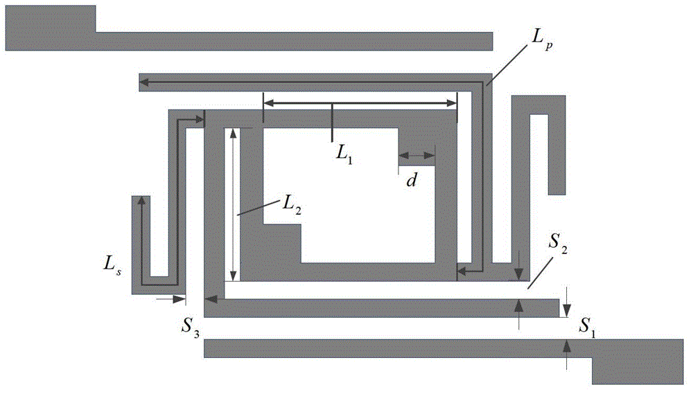
[0066] The square metal ring 4 adopts a microstrip line with a line width of 0.8mm, and its perimeter is 2(L 1 +L 2 )=39.2mm, which is the length of a dielectric waveguide wavelength, corresponding to the center frequency GHz, where L 1 , L 2 is the length of two sides of metal ring 4, and L 1 =11.8mm, L 2 =7.8mm, c is the speed of light in vacuum, ε e is the effective permittivity of the microstrip resonator, f 0 is the resonant frequency of the square metal ring 4;

[0067] The line width of perturbation stub 5 is 0.4mm, and the total length L p =29.6mm, the perturbation stub 5 is used to split the degenerate mode of the metal ring 4, so that the frequency of the three split modes is lower than the resonant frequency f of the metal ring 4 0 , the two modes with lower fre...


PUM


Abstract

The invention discloses a multimode wide-band filter based on a multi-branch loaded square resonance ring, which mainly solves the problem that the circuit size of a conventional multimode wide-band filter is limited by the area of the resonance ring. The filter comprises a micro-band dielectric substrate (1), a metal grounding plate (2), a square resonance ring (3) and a pair of input and output feed lines (8). The square resonance ring (3) comprises a square metal ring (4), a pair of equilong perturbation branches (5), a pair of impedance matching metal pieces (6), and a pair of transmission zero point branches (7). The two equilong perturbation branches (5) are located at a pair of external opposite angles of the square metal ring (4). The two same impedance matching metal pieces (6) are located at the other pair of opposite angles of the metal ring (4). The transmission zero branches (7) and the equilong perturbation branches (5) are connected in parallel or located in the metal ring (4) and are connected with the inner edge of the metal ring (4). The pair of input and output feed lines (8) is symmetrically arranged above the micro-band dielectric substrate (1) horizontally, and is parallel to the tail ends of the perturbation branches. According to the multimode wide-band filter, the circuit size of the filter is reduced, and the circuit is miniature, and the filter can be applied to wireless communication systems.

Description

technical field [0001] The invention belongs to the technical field of electronic devices, and in particular relates to a microstrip multimode wideband filter, which can be used for a radio frequency front end of a wireless communication system. Background technique [0002] With the rapid development of mobile communication, satellite communication, radar, and remote sensing technology, the wireless spectrum is increasingly crowded, which puts forward very strict requirements on the radio frequency microwave filter in the communication system. Microstrip filters have the advantages of small size, light weight, low cost, and easy processing, and are widely used in microwave circuits. There are various types and realization forms of microstrip filters, and the research of miniaturized high-performance microstrip filters has always been a hot field. Traditional filter forms such as Butterworth and Chebyshev filters can only meet high selectivity requirements by increasing the...

Claims


Application Information

Patent Timeline
Patent Type & Authority Applications(China)
IPC IPC(8): H01P1/203H01P7/08
Inventor 邓坤吴边孙守家陈佳王楠史小卫
Owner XIDIAN UNIV
Why Eureka
Try Eureka