Fault simulation system and fault analysis method for single event upset

A single-event flipping and fault simulation technology, applied in the field of single-event flipping fault simulation systems and analysis, can solve problems such as slow simulation speed, and achieve the effects of flexible use, fast simulation speed, and improved simulation speed

CN103198868AInactive Publication Date: 2013-07-10NORTHWEST INST OF NUCLEAR TECH
5 Cites 57 Cited by

Patent Information

Authority / Receiving Office
CN · China
Patent Type
Applications(China)
Current Assignee / Owner
Publication Date
2013-07-10
Estimated Expiration
Not applicable · inactive patent

Smart Images

  • Figure 1
    Figure 1
  • Figure 2
    Figure 2
  • Figure 3
    Figure 3
Patent Text Reader

Abstract

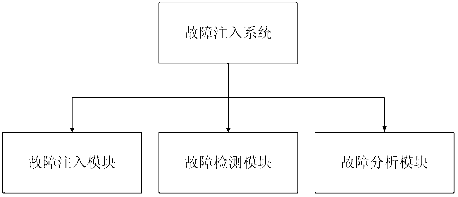
The invention relates to a fault simulation system and a fault analysis method for single event upset in a large scale integrated circuit SRAM-type FPGA (Field Programmable Gate Array). The fault simulation system comprises a host computer and a control board, wherein the control board comprises a fault injection module, a fault detecting module and a fault analyzing module. The fault simulation system and the fault analysis method provided by the invention are flexible to use, low in cost, high in simulation precision, fast in simulation speed and free from any physical damage to a chip.
Need to check novelty before this filing date? Find Prior Art

Description

technical field

[0001] The invention relates to a fault simulation system and analysis method of single event reversal, in particular to a fault simulation system and analysis method for single event reversal in large-scale integrated circuit SRAM type FPGA. Background technique

[0002] When a single high-energy charged particle is incident into the sensitive volume of a semiconductor device, the transient disturbance or permanent damage to the circuit is called single event effect. Electronic systems working on satellites and spacecraft are in the space radiation environment, and appropriate hardening measures must be taken to solve the reliability problems caused by single event effects. Field Programmable Gate Array (FPGA) is a semi-customized digital large-scale integrated circuit. The chip contains rich programmable logic resources and interconnection resources. Users can realize various digital circuit functions through programming and configuration. The circuit struc...

Examples

Embodiment Construction

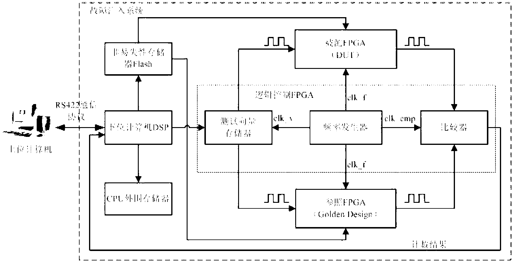
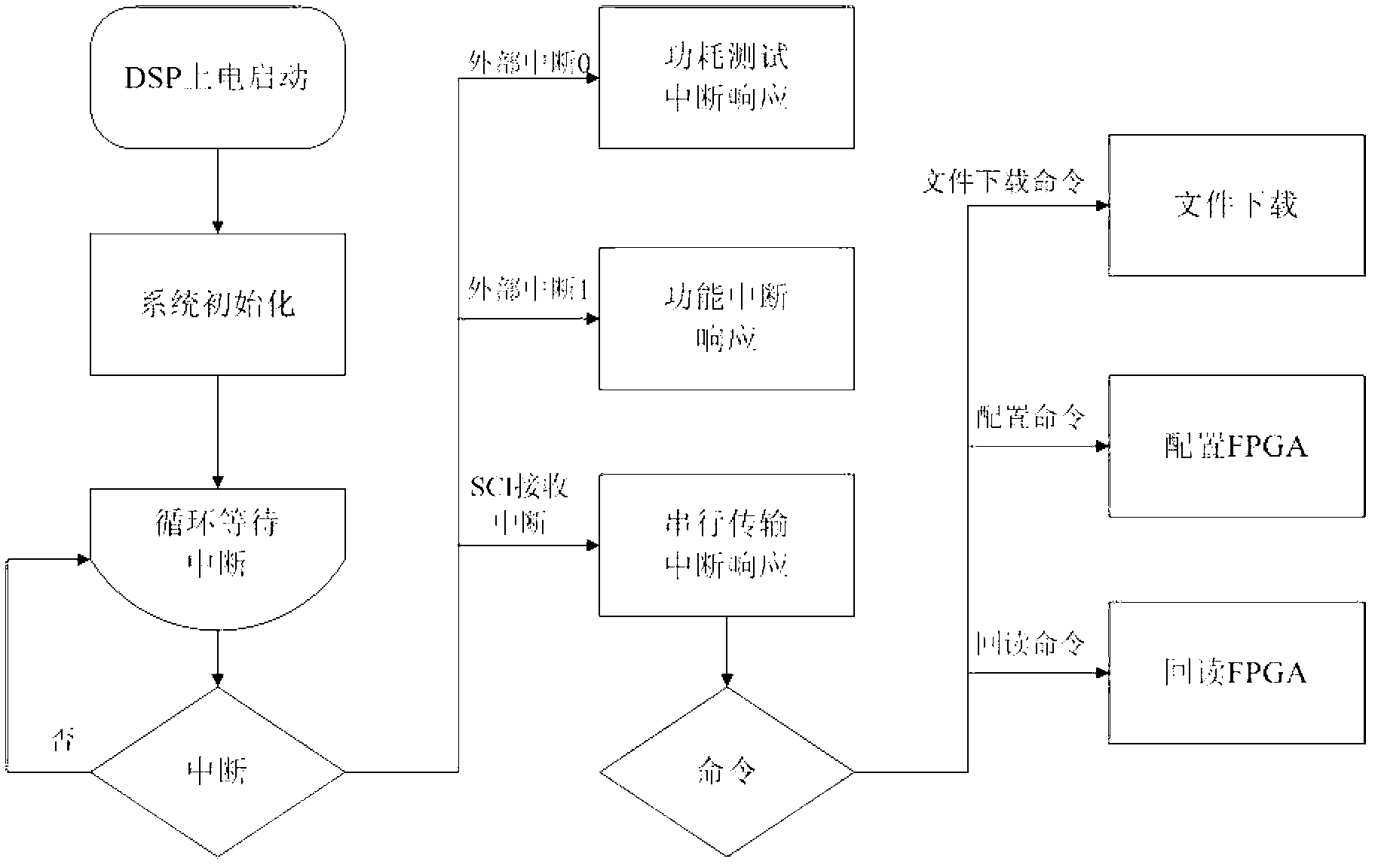
[0050] figure 2 It is a schematic diagram of the hardware structure of the fault injection system in the present invention. The main frame of the system is composed of a host computer and a control board, and the serial port communication protocol RS422 is used for communication between the host computer and the control board. The lower computer adopts TI’s 2000 series DSP TMS320LF2407, which is mainly responsible for receiving commands and data from the upper computer, returning the test data obtained from the test board to the computer, reading and writing Flash, and controlling timing and logic control of the FPGA pair. The FPGA under test is configured and read back.

[0051] The timing and logic control circuit is realized by the Spartan-II series FPGA of Xilinx Company, which is mainly responsible for the realization of the timing and logic control circuit, including: generating the clock signal of the system, such as the synchronous clock of two FPGAs, the output clock...