Production method of metal micro-nano structure based on laser interference induced cross-linking reaction

A technology of laser interference and induced cross-linking, applied in microstructure technology, microstructure devices, manufacturing microstructure devices, etc., can solve problems such as batch preparation and application of unfavorable metal micro-nanostructures, process, equipment, efficiency or quality. , to achieve the effect of low cost, high sample quality and good repeatability

Active Publication Date: 2013-07-17
BEIJING UNIV OF TECH
View PDF8 Cites 1 Cited by
  • Summary
  • Abstract
  • Description
  • Claims
  • Application Information

AI Technical Summary

Problems solved by technology

The traditional fabrication methods of metal micro-nano structures include: electron beam lithography, reactive ion beam etching, nanoimprinting technology, metal colloid solution method,

Method used


Image

  • Production method of metal micro-nano structure based on laser interference induced cross-linking reaction
  • Production method of metal micro-nano structure based on laser interference induced cross-linking reaction
  • Production method of metal micro-nano structure based on laser interference induced cross-linking reaction

Examples


Embodiment 1

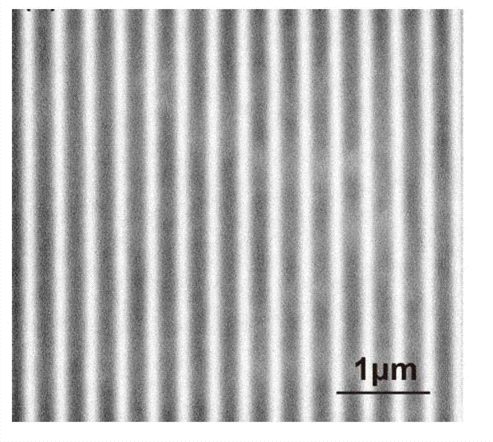
[0019] Example 1: A method for preparing a one-dimensional metal micro-nano structure based on laser interference-induced cross-linking reaction.

[0020] 1) The organic semiconductor material F8BT is dissolved in an organic solvent (the organic solvent is one of xylene, toluene, chlorobenzene, dichlorobenzene, benzene, chloroform, cyclohexane, pentane, hexane or octane ) to make an organic semiconductor solution with a concentration of 25 mg / ml;

[0021] 2) Spin-coat the F8BT solution in step 1) on the substrate at a speed of 2000rpm to prepare an organic semiconductor polymer film with a thickness of 100nm;

[0022] 3) Evaporating a layer of metal film with a thickness of 10nm on the organic semiconductor polymer film in step 2);

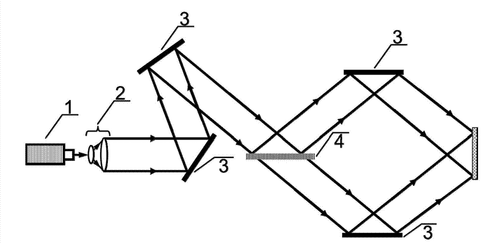
[0023] 4) The one-dimensional laser interference light field (laser wavelength is 325nm) interacts with the continuous organic semiconductor polymer film to cause cross-linking reaction of the polymer material and pattern the metal film attached ...

Embodiment 2

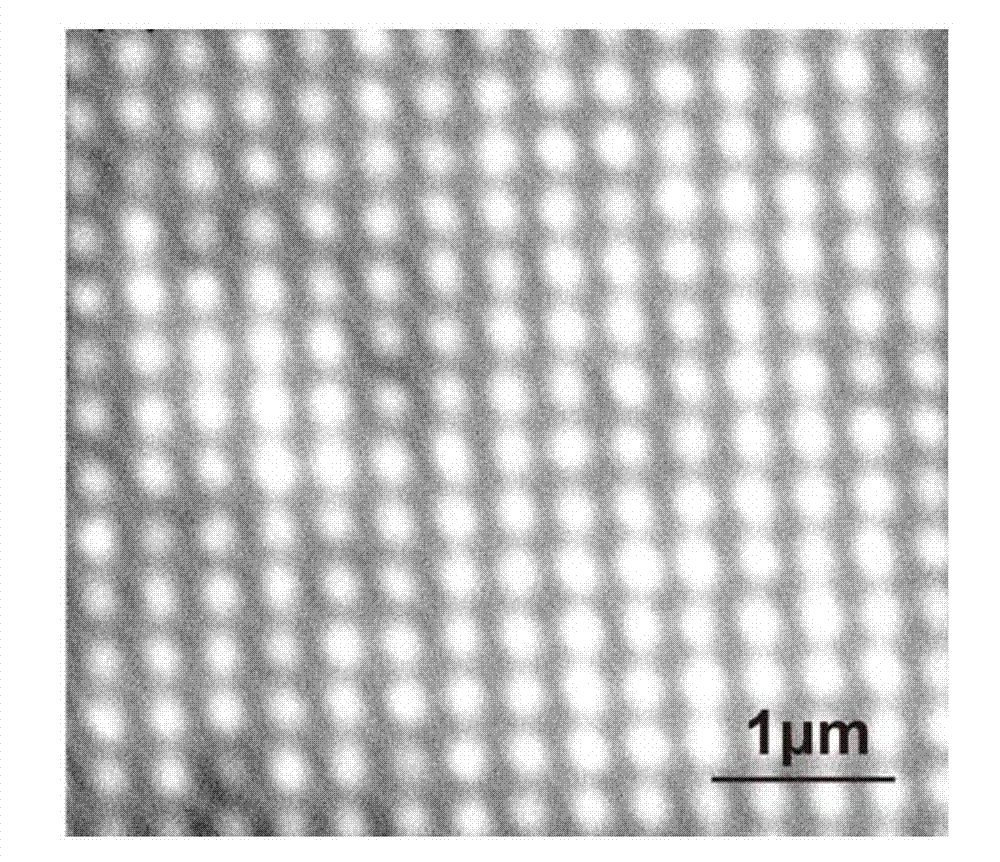
[0024] Example 2: A method for preparing a two-dimensional metal micro-nano structure based on laser interference-induced cross-linking reaction.

[0025] 1) The organic semiconductor material F8BT is dissolved in an organic solvent (the organic solvent is one of xylene, toluene, chlorobenzene, dichlorobenzene, benzene, chloroform, cyclohexane, pentane, hexane or octane ) to make an organic semiconductor solution with a concentration of 25mg / ml;

[0026] 2) Spin-coat the F8BT solution in step 1) on the substrate at a speed of 2000rpm to prepare an organic semiconductor polymer film with a thickness of 100nm;

[0027] 3) Evaporating a layer of metal film with a thickness of 10nm on the organic semiconductor polymer film in step 2);

[0028] 4) The two-dimensional laser interference light field (laser wavelength is 458nm) interacts with the continuous organic semiconductor polymer film to cause a cross-linking reaction of the polymer material and pattern the metal film attached...


PUM

PropertyMeasurementUnit
Thicknessaaaaaaaaaa

Abstract

The invention discloses a production method of a metal micro-nano structure based on laser interference induced cross-linking reaction and belongs to the technical field of optoelectronic materials and devices. The production technique includes: subjecting polymers to cross-linking reaction through organic semiconductor polymer material coated with a metal film by laser irradiation, forming a surface relief structure, and texturizing the attached metal film. The production method has the advantages of low cost, high efficiency, capability of producing large-area metal structures with plasma resonance spectral response, and the like.

Description

technical field [0001] The invention belongs to the technical field of metal micro-nano structure preparation, and uses a laser interference light field to irradiate an organic semiconductor polymer material coated with a metal film to prepare a large-area metal micro-nano structure with plasmon resonance spectral response. Background technique [0002] Fabrication of large-area metal micro-nanostructures at low cost is a research topic that is widely concerned in the world, and it is of great significance in practical applications. The traditional fabrication methods of metal micro-nano structures include: electron beam lithography, reactive ion beam etching, nanoimprinting technology, metal colloid solution method, etc., but these methods have deficiencies in process, equipment, efficiency or quality, which are not conducive to metal Practical batch preparation and application of micro-nanostructures. The method of preparing metal micro-nanostructures based on laser inter...

Claims


Application Information

Patent Timeline
IPC IPC(8): B81C1/00
Inventor 翟天瑞林远海张新平刘红梅王丽
Owner BEIJING UNIV OF TECH
Why Eureka
Try Eureka