Imaging array of pixel units based on composite dielectric grid structure and exposure operation method of imaging array

A pixel unit and composite medium technology, applied in the direction of electrical components, image communication, color TV components, etc., can solve the problems that the pixel size is difficult to further reduce, the yield and cost are not ideal, and the sensitivity and resolution are small. Achieve the effects of preventing crosstalk, increasing the density of imaging devices, and improving resolution

Active Publication Date: 2013-07-31
NANJING UNIV
View PDF4 Cites 6 Cited by
  • Summary
  • Abstract
  • Description
  • Claims
  • Application Information

AI Technical Summary

Problems solved by technology

CMOS-APS has received more attention in recent years due to some advantages. CCD production has extremely high requirements on technology, and the yield and cost are not ideal.
At present, both CCD and CMOS are trying to further reduce the pixel size and improve the resolution. CCD is difficult to further reduce the pixel size due to the effects of fringe electric field and other effects.
In CMOS-APS, each pixel is composed of multiple transistors and a photosensitive diode, so that the photosensitive area of ​​each pixel only occupies a small surface area of ​​the pixel itself, and the sensitivity and resolution are relatively small.
In addition, each pixel of CMOS-APS contains multiple transistors to complete operations such as address gating, and a general pixel unit contains three transistors, which determines that its pixel size is greatly limited.

Method used


Image

  • Imaging array of pixel units based on composite dielectric grid structure and exposure operation method of imaging array
  • Imaging array of pixel units based on composite dielectric grid structure and exposure operation method of imaging array
  • Imaging array of pixel units based on composite dielectric grid structure and exposure operation method of imaging array

Examples


Embodiment Construction

[0020] The structure of the detector of the present invention and its specific detection method will be described below with reference to the accompanying drawings.

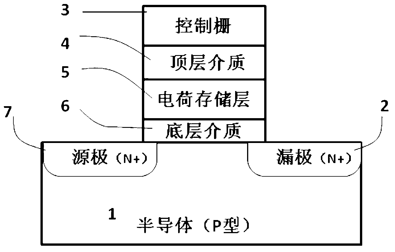
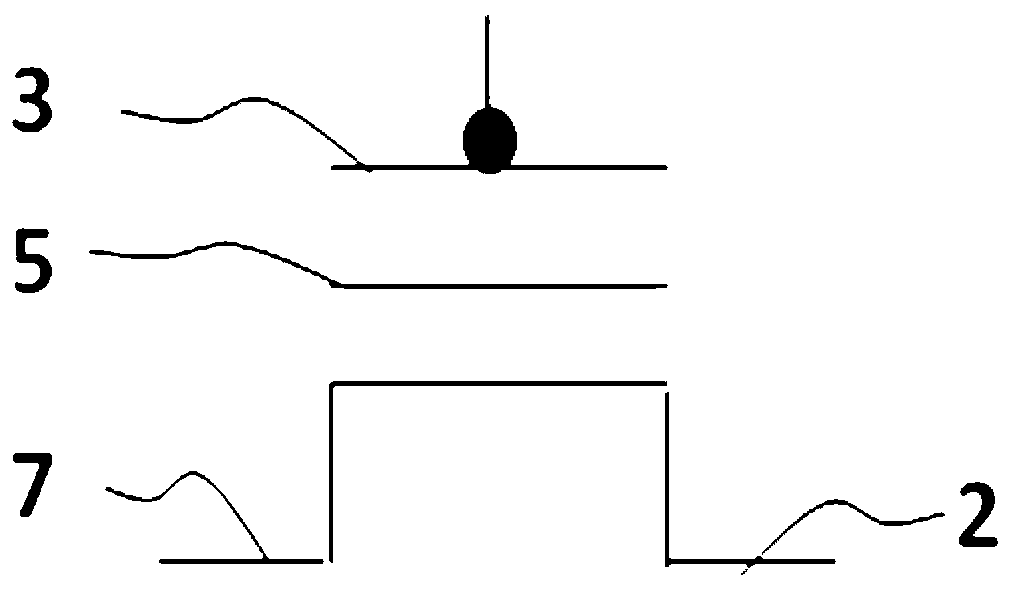
[0021] The present invention is based on the basic structure of the pixel involved in the imaging array of the composite dielectric grid structure pixel unit and its exposure operation method, such as Figure 1a Shown is the pixel structure (refer to WO2010 / 094233, the thickness of the dielectric material can be referred to), including a P-type semiconductor substrate (1), an N-type drain region (2), and an N-type source region (7). From top to bottom, there are a control gate (3), a top dielectric (4), a charge storage layer (5), and a bottom dielectric (6). Figure 1b It is a representation diagram of a pixel structure circuit, (3) a gate, (5) a charge storage layer, (2) and (7) are N-type injection regions with a symmetrical structure.

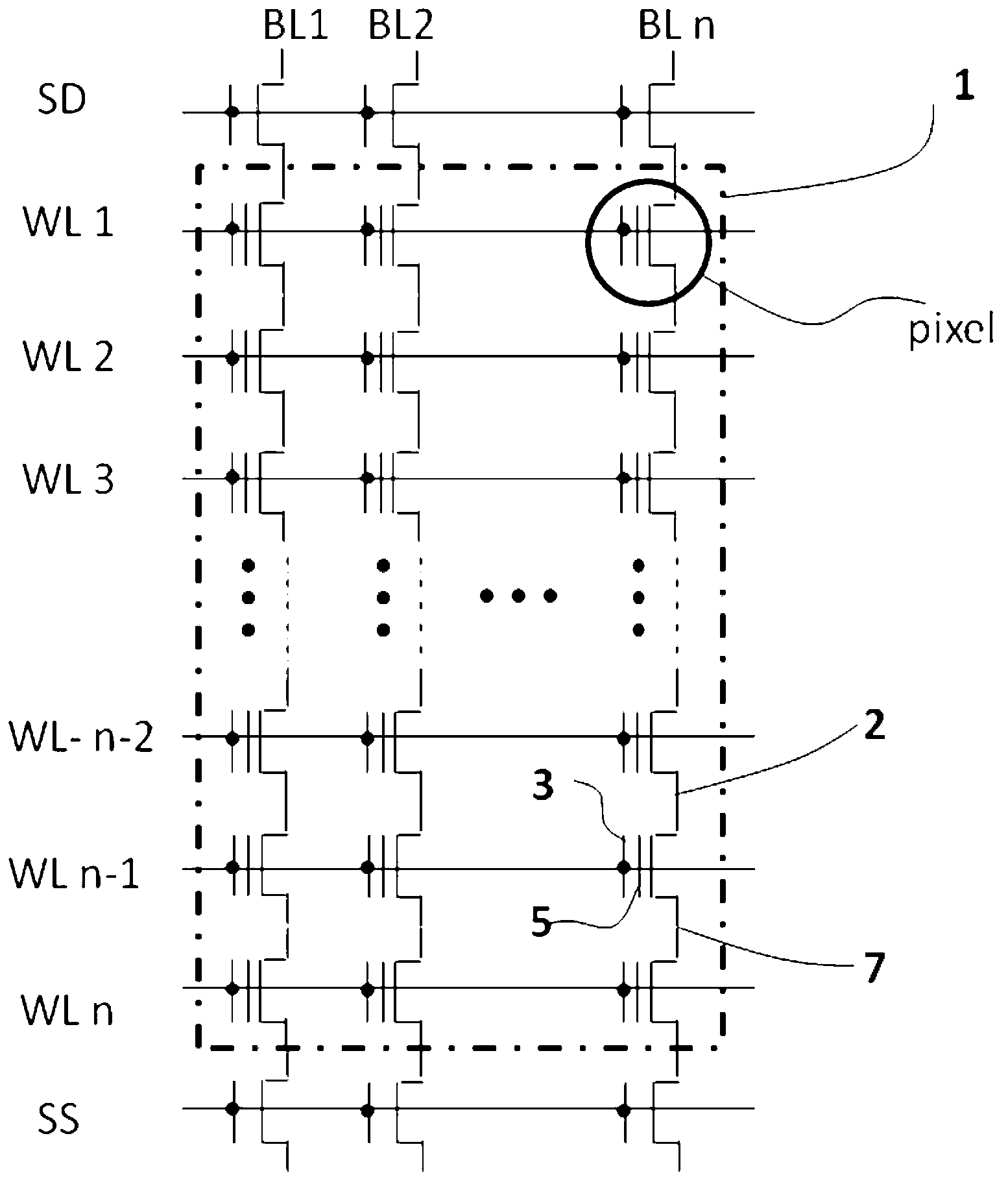
[0022] The basic structure of the imaging array based on the compound die...


PUM


Abstract

The invention provides an imaging array of pixel units based on a composite dielectric grid structure and an exposure operation method of the imaging array. The pixel units adopt light-sensitive detectors in composite dielectric grid structures; a source region and a drain region of each pixel unit are symmetrical; a P-type substrate (1) is formed by injection; an N-type injection region is arranged between every two adjacent pixel units to form a pixel shared drain electrode (2) or a source electrode (7); the pixel units are mutually connected in series by the N-type injection regions to form lines; two selective switch transistors are arranged at the two ends of each line (BL); drain electrode directions of grid control ports of the transistors are SD; source electrode directions are SS; transmission of signals of each line and selective on of each line are controlled by controlling switches of the selective transistors; each row of different pixels in each line connects grid electrodes (3) with a word line (WL); and each WL simultaneously controls the grid electrodes of each row of pixels.

Description

technical field [0001] The invention relates to a compound dielectric gate structure pixel unit, in particular to a NAND imaging array structure, which is a NAND array structure composed of a compound dielectric gate pixel unit and an exposure operation method. Background technique [0002] Image sensors are widely used in today's society, such as mobile phones, digital cameras, various video cameras, and national defense detection fields. The main imaging detectors currently developed are CCD and CMOS-APS. The basic structure of CCD is a series of MOS capacitors. In series, the generation and change of the potential well on the semiconductor surface is controlled by the timing of the voltage pulse on the capacitor, so as to realize the storage and transfer readout of the photogenerated charge signal. Each pixel of CMOS-APS is composed of diodes and multiple transistors to read the changes before and after exposure get light signal. CMOS-APS has received more attention in r...

Claims


Application Information

Patent Timeline
Patent Type & Authority Applications(China)
IPC IPC(8): H01L27/146H04N5/335
Inventor 闫锋夏好广卜晓峰吴福伟马浩文司向东
Owner NANJING UNIV
Why Eureka
Try Eureka