Hollow channel isolation region preparation method

A shallow trench isolation and manufacturing method technology, which is applied in the field of shallow trench isolation, can solve problems affecting device characteristics, etching residues, increasing the difficulty of etching polysilicon gates and silicon nitride sidewalls, etc. Achieve the effect of solving edge corners or sags, improving appearance, and facilitating subsequent processes

Inactive Publication Date: 2013-08-14
SHANGHAI HUALI MICROELECTRONICS CORP
View PDF2 Cites 2 Cited by
  • Summary
  • Abstract
  • Description
  • Claims
  • Application Information

AI Technical Summary

Problems solved by technology

However, STI also has many technical problems in the process, such as the shape control of STI, the rounding of the top corner of STI, the adaptation stress between the silicon dioxide inside the STI and the external silicon, and the defect of the top edge of the shallow trench isolation region. Corner problem (STIDivot), etc.
Among them, the problem caused by the notch at the top edge of the shallow trench isolation region will be directly related to the leakage problem at the edge of the STI, which will affect the characteristics of the device. When an inversion layer is formed on the side of the active region, it will cause a parasitic current path, which will affect the characteristics of the device, and the notch at the top edge of the too deep shallow trench isolation region will increase the etching of the polysilicon gate and silicon nitride sidewall Therefore, controlling the size and depth of the notch at the top edge of the shallow trench isolation region has attracted more and more attention.

Method used


Image

  • Hollow channel isolation region preparation method
  • Hollow channel isolation region preparation method
  • Hollow channel isolation region preparation method

Examples


no. 1 example

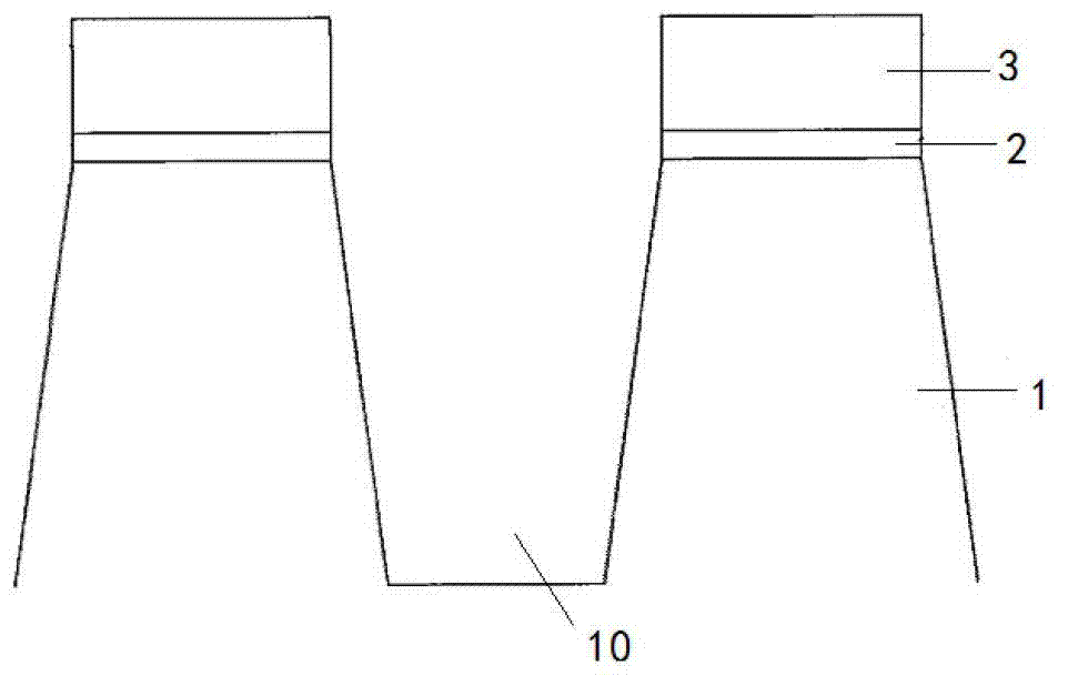
[0028] see Figure 1 to Figure 6 , the manufacturing method of the shallow trench isolation region of the present embodiment includes the following steps:

[0029] Step S01, providing a silicon substrate 1, and sequentially depositing SiO with a thickness of 15 nanometers on the silicon substrate 1 2 Layer 2 and SiN layer 3 with a thickness of 80 nanometers, and shallow trenches 10 are etched by STI manufacturing process;

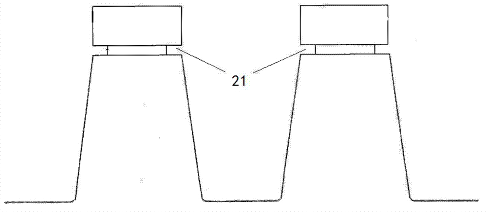
[0030] Step S02, on the SiO on both sides of the shallow trench 10 2 Layer 2 cuts are etched, and the etching width is 14 nanometers, forming a groove 21;

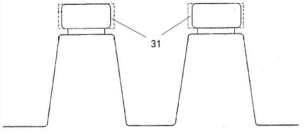
[0031] Step S03, perform the first etching back on the SiN layer 3 on both sides of the shallow trench 10, remove the first part of the SiN layer 31, the width of the etching back is 8 nanometers, and expose the bottom of the SiN layer 3 from the projection direction from top to bottom Part of the silicon substrate 1 below the groove 21;

[0032] Step S04, growing a layer of SiO on the surface of th...


PUM


Abstract

The invention discloses a hollow channel isolation region preparation method which comprises the following steps: providing a supporting base; sequentially depositing buffering oxide layers and nitride layers on the supporting base; etching a hollow channel by utilizing the shallow trench isolation (STI) manufacturing technique; etching buffering oxide layer cuts on two sides of the shallow channel to form a groove; performing the first etching on the nitride layers on two sides of the shallow channel; growing a layer of oxidation film on the surface of the supporting base; and performing the second etching on the nitride layers on two sides of the shallow channel. The method starts from morphology of nitrides and realizes performance improvement of devices through modification of fewer craft processes, and utilizes twice etching to improve morphology of silicon nitride, so that the problem that the shallow channel isolation top edge lacks corners or hollows after the silicon nitride is removed is solved; and at the same time, the outline of corners of the shallow channel isolation region can be improved, so that the subsequent handling is facilitated.

Description

technical field [0001] The invention relates to the field of semiconductor manufacturing, in particular to a method for manufacturing a shallow trench isolation region. Background technique [0002] In recent years, with the development of semiconductor integrated circuit manufacturing technology, the number of components contained in the chip has been increasing, and the size of the components has been continuously reduced due to the improvement of integration. The line width used in the production line has entered the sub-micron level. scope. However, no matter how the device size is reduced, there must still be proper insulation or isolation between the various devices in the chip in order to obtain good device properties. The technology in this area is generally called Device Isolation Technology (Device Isolation Technology), and its main purpose is to form spacers between the components, and to ensure good isolation effect, minimize the area of ​​the spacers to free u...

Claims


Application Information

Patent Timeline
Patent Type & Authority Applications(China)
IPC IPC(8): H01L21/762
Inventor 陈佳旅张幼杰曹亚民
Owner SHANGHAI HUALI MICROELECTRONICS CORP
Why Eureka
Try Eureka