Double-grid electric charge capturing memory and manufacture method thereof

A technology of charge trapping and manufacturing method, which is applied in the field of microelectronics, can solve the problems of losing information, affecting data access speed, and charge loss, and achieves the effects of dense distribution of thresholds, improving programming and erasing speed, and increasing turn-on current

Active Publication Date: 2015-06-17
INST OF MICROELECTRONICS CHINESE ACAD OF SCI
View PDF3 Cites 0 Cited by
  • Summary
  • Abstract
  • Description
  • Claims
  • Application Information

AI Technical Summary

Problems solved by technology

However, due to the continuous distribution of the bound charges in the floating gate, if there is a charge leakage phenomenon in the part of the device, all the charges in the entire device will be lost, thereby losing the stored information.
In order to improve the data retention and reliability of the device, it is necessary to ensure that the silicon-based oxide that wraps the floating gate layer cannot leak charges. The main way is to increase the thickness of the oxide, but this will affect the data access speed.

Method used


Image

  • Double-grid electric charge capturing memory and manufacture method thereof
  • Double-grid electric charge capturing memory and manufacture method thereof
  • Double-grid electric charge capturing memory and manufacture method thereof

Examples


Embodiment Construction

[0034] In order to make the object, technical solution and advantages of the present invention clearer, the present invention will be described in further detail below in conjunction with specific embodiments and with reference to the accompanying drawings.

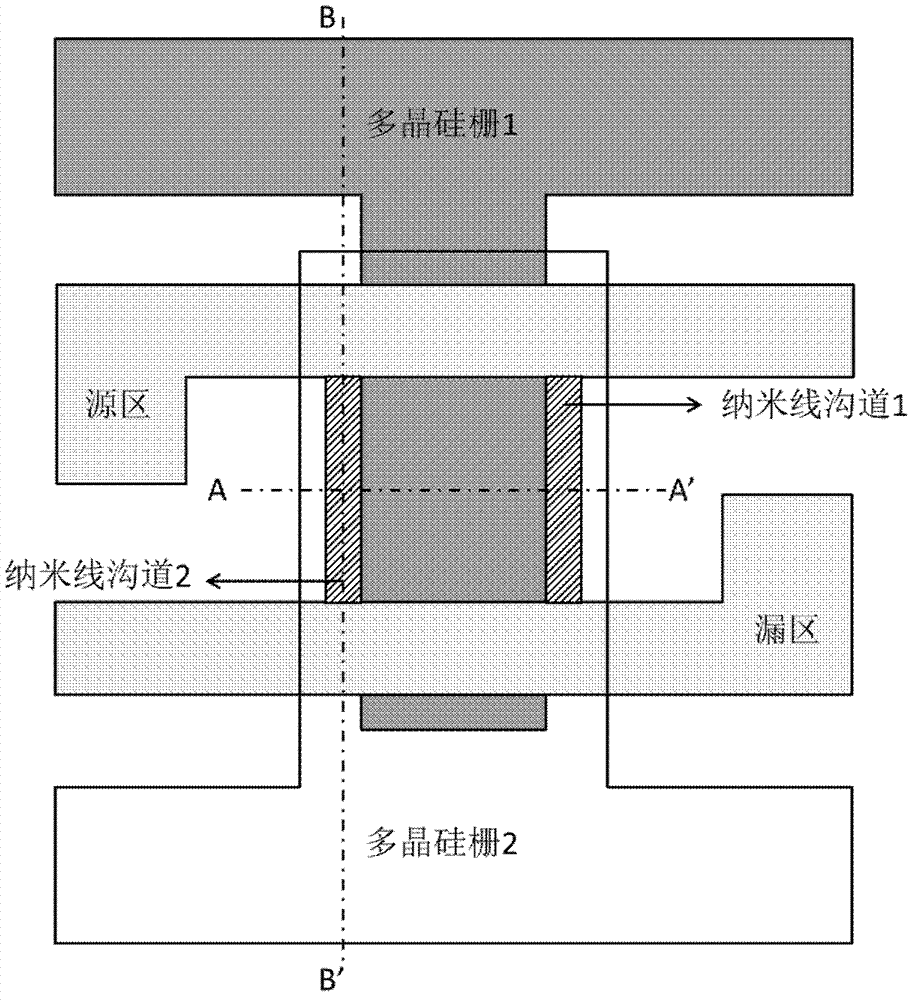
[0035] figure 1 It is a top view structural diagram of a double-gate charge trapping memory based on a polysilicon nanowire field effect transistor according to an embodiment of the present invention. From figure 1 It can be seen in the figure that there are two independent polysilicon gates in the device structure, which are polysilicon gate 1 on the bottom layer of the device and polysilicon gate 2 on the top layer of the device, and the two gates between the two gates are on both sides of polysilicon gate 1 Symmetrically distributed polysilicon nanowires constitute the channel portion of the device. The source region and the drain region of the device pass through the overlapping part between the two gates, connect w...


PUM


Abstract

The invention relates to a double-grid electric charge capturing memory based on a polycrystalline silicon nanowire field effect transistor and a manufacture method thereof. The double-grid electric charge capturing memory is provided with two polycrystalline silicon grid electrodes, and comprises a semiconductor substrate, a first dielectric buffer layer formed on the semiconductor substrate, a second dielectric buffer layer formed on the first dielectric buffer layer, a polycrystalline silicon bottom grid formed on the second dielectric buffer layer, two nanowire channels symmetrically distributed on the two sides of the polycrystalline silicon bottom grid, two electric charge capturing memory dielectric layers formed between the polycrystalline silicon bottom grid and the nanowire channels respectively, two top grid dielectric layers formed on the outer side of the two nanowire channels, a hard masking layer formed on the polycrystalline silicon bottom grid, the electric charge capturing memory dielectric layers, the nanowire channels and the top grid dielectric layers, a polycrystalline silicon top grid formed on the hard masking layer and the electric charge capturing memory dielectric layers and a source region and a drain region, spanning the two nanowire channels.

Description

technical field [0001] The invention relates to the technical field of microelectronics, in particular to a double-gate charge-trapping memory based on a polysilicon nanowire field-effect transistor and a manufacturing method thereof. Background technique [0002] Flash storage technology is a mainstream storage technology now. It not only has the advantages of random access memory (RAM), which can erase and rewrite data information at any time, but also has the characteristics of read-only memory (ROM). The stored data information is kept under certain circumstances, so flash memory is also called a non-volatile memory. [0003] The mainstream flash storage technology can be divided into two categories according to the array structure and realized functions: the flash storage technology of the NAND array architecture and the flash storage technology of the NOR array architecture. The former mainly focuses on the preservation of large-capacity data information, while the la...

Claims


Application Information

Patent Timeline
Patent Type & Authority Patents(China)
IPC IPC(8): H01L29/10H01L27/115H01L21/8247
Inventor 刘明王晨杰霍宗亮张满红刘璟王永谢常青
Owner INST OF MICROELECTRONICS CHINESE ACAD OF SCI
Why Eureka
Try Eureka