Method of growing a high quality iii-v compound layer on a silicon substrate

A III-V, compound technology, applied in the field of semiconductor manufacturing, can solve problems such as fragmentation defects, low quality, wafer defects, etc.

Active Publication Date: 2013-08-21
EPISTAR CORP
View PDF5 Cites 24 Cited by
  • Summary
  • Abstract
  • Description
  • Claims
  • Application Information

AI Technical Summary

Problems solved by technology

However, existing methods of forming III-V compound layers on silicon substrates may cause wafer defects (e.g., chipping) due to the lattice constant mismatch between the III-V compound layers and the silicon substrate. defects) or produce low-quality III-V compound layers
[0004] Thus, while existing methods of forming III-V compound layers on silicon substrates are generally adequate for their intended purposes, they are not entirely satisfactory in all respects.

Method used


Image

  • Method of growing a high quality iii-v compound layer on a silicon substrate
  • Method of growing a high quality iii-v compound layer on a silicon substrate
  • Method of growing a high quality iii-v compound layer on a silicon substrate

Examples


Embodiment Construction

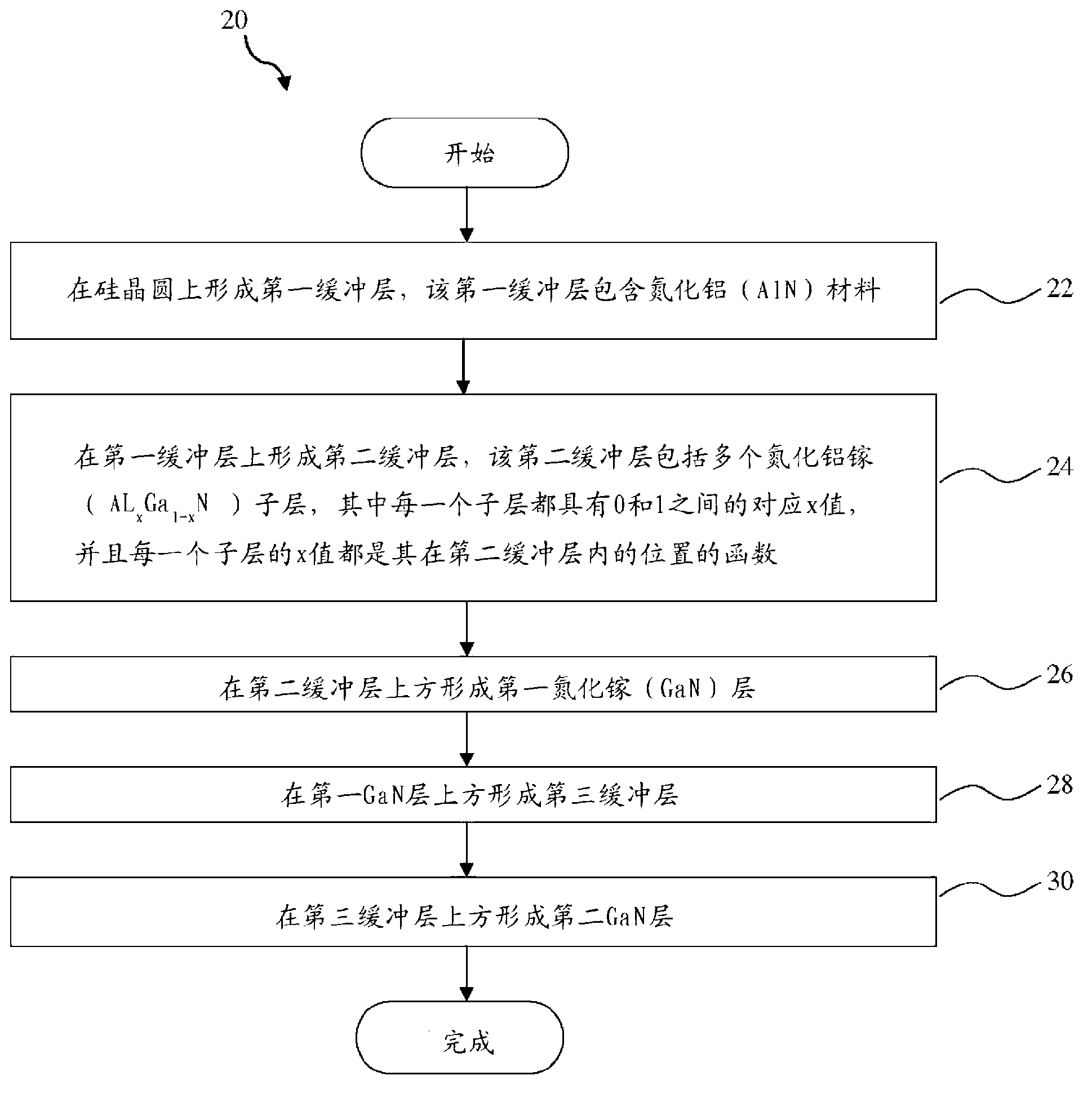
[0030] It should be appreciated that the following disclosure provides many different embodiments, or examples, for implementing different elements of the various embodiments of the invention. Specific examples of components and arrangements are described below to simplify the present disclosure. These are of course merely examples and are not intended to be limiting. For example, the formation of a first component over or on a second component in the following description may include embodiments in which the first and second components are formed in direct contact, and may also include embodiments in which the first and second components may be formed in direct contact. An embodiment in which an additional part is formed between the second parts such that the first and second parts are not in direct contact. Furthermore, the terms "top", "bottom", "below", "above", etc. are used for convenience and are not meant to limit the scope of the embodiments to any particular orienta...


PUM

PropertyMeasurementUnit
thicknessaaaaaaaaaa
thicknessaaaaaaaaaa
thicknessaaaaaaaaaa

Abstract

The present disclosure involves a method of fabricating a semiconductor device. A surface of a silicon wafer is cleaned. A first buffer layer is then epitaxially grown on the silicon wafer. The first buffer layer contains an aluminum nitride (AlN) material. A second buffer layer is then epitaxially grown on the first buffer layer. The second buffer layer includes a plurality of aluminum gallium nitride (AlxGa1-xN) sub-layers. Each of the sub-layers has a respective value for x that is between 0 and 1. A value of x for each sub-layer is a function of its position within the second buffer layer. A first gallium nitride (GaN) layer is epitaxially grown over the second buffer layer. A third buffer layer is then epitaxially grown over the first GaN layer. A second GaN layer is then epitaxially grown over the third buffer layer.

Description

technical field [0001] The present invention relates generally to semiconductor fabrication, and more specifically to growing high quality III-V compound layers over silicon substrates. Background technique [0002] In recent years, the semiconductor integrated circuit (IC) industry has experienced rapid growth. Technological advancements in IC materials and design have produced various types of ICs for different purposes. The fabrication of some types of ICs may require the formation of a III-V compound layer on a substrate, for example, a gallium nitride layer on the substrate. These types of IC devices may include, for example, light emitting diode (LED) devices, radio frequency (RF) devices, high electron mobility transistor (HEMT) devices, and high power semiconductor devices. [0003] In traditional processes, manufacturers typically form III-V compound layers on sapphire substrates. However, sapphire substrates are expensive. As a result, some manufacturers have b...

Claims


Application Information

Patent Timeline
Patent Type & Authority Applications(China)
IPC IPC(8): H01L29/205H01L21/02H01L21/20H01L33/00
CPCH01L21/0254H01L21/02052H01L21/02381H01L21/02458H01L21/02505H01L21/0262H01L29/1075H01L29/20H01L29/2003H01L29/66462H01L29/7787H01L33/007H01L33/12
Inventor 李镇宇夏兴国郭浩中
Owner EPISTAR CORP
Why Eureka
Try Eureka