1300nm-1550nm semiconductor laser unit containing bismuthide and preparation method thereof

A laser and semiconductor technology, applied in the direction of semiconductor lasers, lasers, laser parts, etc., can solve the problems of high non-radiative recombination rate, increase the difficulty of growth process, deterioration of laser performance, etc., to improve the injection efficiency, reduce the difficulty of growth process, The effect of high characteristic temperature

Active Publication Date: 2013-08-21
SUZHOU INST OF NANO TECH & NANO BIONICS CHINESE ACEDEMY OF SCI
View PDF3 Cites 11 Cited by
  • Summary
  • Abstract
  • Description
  • Claims
  • Application Information

AI Technical Summary

Problems solved by technology

So far, for the InGaNAs / GaAs material system, it is still difficult to increase the N content to 10%, and doping N atoms is easy to introduce defects, so the laser based on this material system is still in the basic stage
For the InAlGaAs / InP material system, it is well known that the higher oxidation rate of Al atoms will not only increase the difficulty of the growth process, but also bring about a higher non-radiative recombination rate, resulting in deterioration of laser performance
Therefore, the lifetime and reliability of lasers containing Al in the active area are inferior to those of lasers without Al in the active area

Method used


Image

  • 1300nm-1550nm semiconductor laser unit containing bismuthide and preparation method thereof

Examples


preparation example Construction

[0073] The preparation method of the 1300nm~1550nm bismuth-containing semiconductor laser is characterized in that the method comprises the following steps:

[0074] Step 1: The 1300nm-1550nm bismuth-containing semiconductor lasers are grown sequentially in the following order:

[0075] (1): growing an N-type AlGaAs transition layer on an N-type GaAs substrate;

[0076] (2): Growth of N-type AlGaAs or GaInP lower confinement layer;

[0077] (3): growing the AlGaAs lower waveguide layer;

[0078] (4): Growth of GaNAsBi / GaAs strained quantum well active region;

[0079] (5): growing the AlGaAs upper waveguide layer;

[0080] (6): growing a P-type AlGaAs electron blocking layer;

[0081] (7): growing a P-type AlGaAs upper confinement layer corresponding to the N-type AlGaAs lower confinement layer, or a P-type GaInP upper confinement layer corresponding to the N-type GaInP lower confinement layer;

[0082] (8): growing a P-type GaAs ohmic contact layer;

[0083] Step 2: The...

Embodiment 1

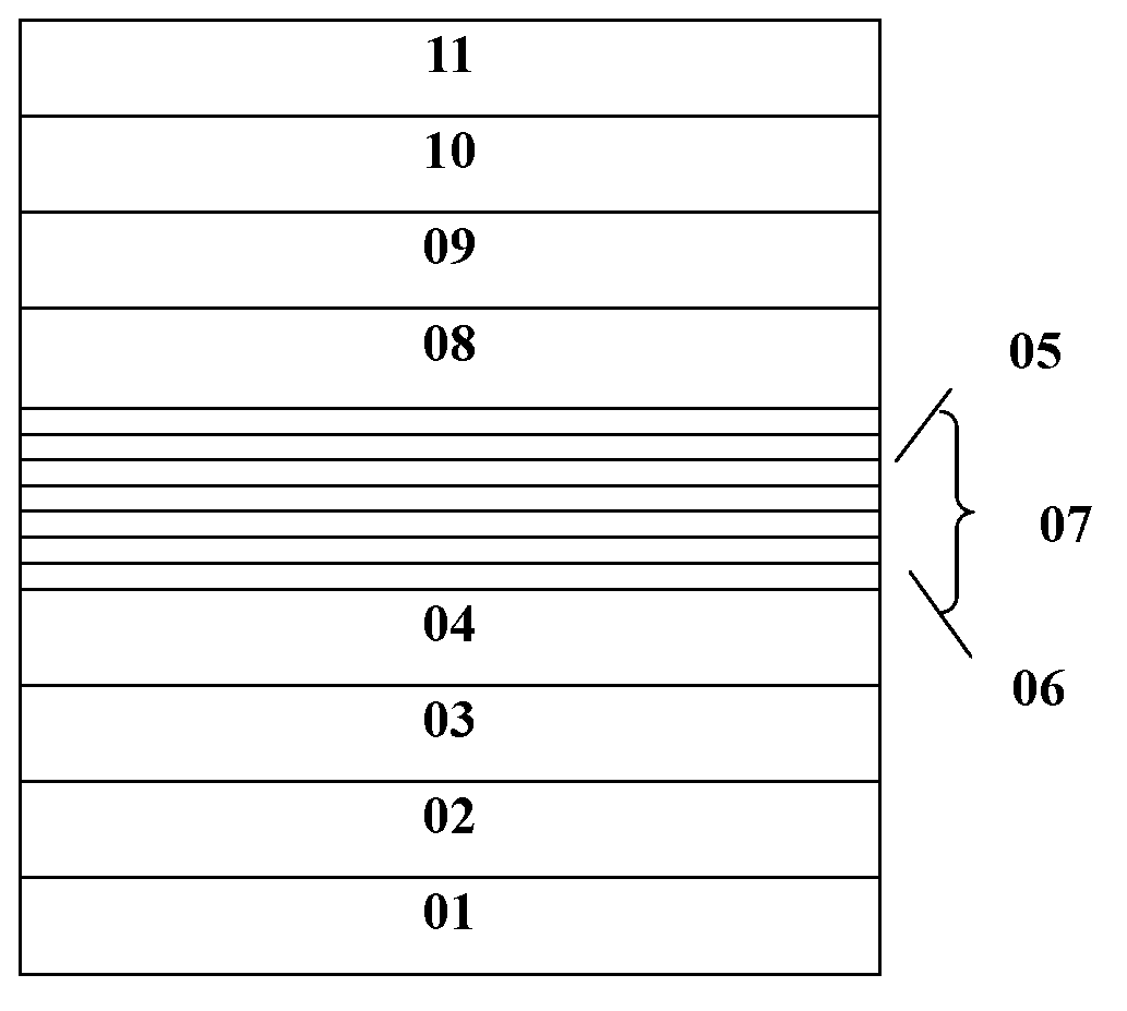
[0095] Embodiment one: if figure 1 , when using AlGaAs as the upper and lower confinement layers, the preparation method of the 1300nm~1.55μm bismuth-containing semiconductor laser comprises the following steps:

[0096] (1) grow the described 1300nm~1550nm bismuth-containing semiconductor laser with MOCVD method, its structure is as follows figure 1 Shown:

[0097] (1) N-type doping is grown on N-type GaAs substrate 01 with about 2×10 18 cm -3 The 0.05 micron AlGaAs layer, the Al composition is gradually changed from 0.1% to 10%, forming a transition layer 02;

[0098] (2) Grow N-type doped about 2×10 18 cm -3 A 0.2 micron AlGaAs layer with an Al composition of 15% forms the lower confinement layer 03;

[0099] (3) Grow a non-doped 0.1 micron AlGaAs composition gradient layer, and the Al composition is gradually changed from 15% to 0.1%, forming the lower waveguide layer 04;

[0100](4) Alternately grow 10nm GaAs barrier layer 05 (4 pieces) and 5.5nm GaNAsBi potential ...

Embodiment 2

[0107] Embodiment 2: as figure 1 , when using GaInP as the upper and lower confinement layers, the preparation method of the 1300nm~1.55μm bismuth-containing semiconductor laser comprises the following steps:

[0108] (1) Growth of 1300nm-1550nm bismuth-containing semiconductor lasers by MOCVD method, the structure of which is as follows figure 1 Shown:

[0109] (1) N-type doping is grown on N-type GaAs substrate 01 with about 2×10 18 cm -3 The 0.05 micron AlGaAs layer, the Al composition is gradually changed from 0.1% to 10%, forming a transition layer 02;

[0110] (2) Grow N-type doped about 2×10 18 cm -3 The 0.2 micron GaInP layer, the composition of Ga is 52%, forms the lower confinement layer 03;

[0111] (3) Grow a non-doped 0.1 micron AlGaAs composition gradient layer, and the Al composition is gradually changed from 15% to 0.1%, forming the lower waveguide layer 04;

[0112] (4) Alternately grow 10nm GaAs barrier layer 05 (4 pieces) and 5.5nm GaNAsBi potential w...


PUM


Abstract

The invention discloses a 1300nm-1550nm semiconductor laser unit containing bismuthide. The 1300nm-1500nm semiconductor laser unit containing bismuthide comprises a transitional layer, a lower limiting layer, a lower waveguide layer, an active area, an upper waveguide layer, an electron barrier layer, an upper limiting layer and an ohmic contacting layer all of which are connected sequentially. The active area adopts a strained quantum well made of a GaNAsBi/ GaAs material system. The P-type AlGaAs electron barrier layer is placed between the P-type AlGaAs upper waveguide layer and the P-type AlGaAs or GaInP upper limiting layer, and the N-type AlGaAs transitional layer is placed between a GaAs substrate and the N-type AlGaAs or GaInP lower limiting layer. A semiconductor laser epitaxy structure grows on the GaAs substrate, the production cost of the semiconductor laser epitaxy structure is less than that of an InP substrate laser, has high feature temperature, can effectively keep a current carrier from overflowing the active area, and can be popularized to a vertical cavity surface emitting laser and other types of lasers.

Description

【Technical field】 [0001] The invention relates to the field of semiconductor optoelectronics, in particular to a 1300nm-1550nm bismuth-containing semiconductor laser and a preparation method thereof. 【Background technique】 [0002] Modern telephone and data networks rely on silicon optical fibers to carry data over the fibers that link the sending and receiving ends. Since silicon optical fiber transmits optical signals in the optical band centered on 1300nm-1550nm, especially 1310nm, it can greatly overcome the dispersion limitation. Therefore, the best working band for the existing local area switching access optical fiber network is at 1310nm. The biggest difficulty encountered in the development of optical fiber communication system lies in the light source. International standards for communication loop networks establish stringent technical parameters for laser diodes or other equivalent light emitting components. These parameters include: the threshold current, at w...

Claims


Application Information

Patent Timeline
Patent Type & Authority Applications(China)
IPC IPC(8): H01S5/343
Inventor 曾徐路董建荣李奎龙孙玉润于淑珍赵勇明赵春雨杨辉
Owner SUZHOU INST OF NANO TECH & NANO BIONICS CHINESE ACEDEMY OF SCI
Why Eureka
Try Eureka