Method for reducing warping stress of LED epitaxy

A warpage stress and epitaxy technology, which is applied in the direction of electrical components, circuits, semiconductor devices, etc., can solve the problems of reducing the warpage stress of LED epitaxy, aggravating the degree of epitaxy warping of epitaxial wafers, and lattice mismatch, so as to improve the wavelength Yield rate, improvement of wavelength uniformity, and effect of warpage improvement

Inactive Publication Date: 2013-09-11
EPILIGHT TECH
View PDF5 Cites 28 Cited by
  • Summary
  • Abstract
  • Description
  • Claims
  • Application Information

AI Technical Summary

Problems solved by technology

[0005] In view of the shortcomings of the prior art described above, the purpose of the present invention is to provide a method for reducing the warping stress of the LED epitaxy, which is used to solve the lattice mismatch and thermal deformation between the sapphire substrate and the GaN epitaxy in the prior art The stress generated by the difference causes the GaN epitaxial wafer to warp, which increases the degree of epitaxial warping when the epitaxial wafer grows the light-emitting layer, reduces the wavelength uniformity of the epitaxial wafer, and leads to a significant drop in the wavelength yield of the epitaxial wafer.

Method used


Image

  • Method for reducing warping stress of LED epitaxy
  • Method for reducing warping stress of LED epitaxy
  • Method for reducing warping stress of LED epitaxy

Examples


Embodiment 1

[0035] Such as Figure 1 to Figure 3 As shown, the present invention provides a method for reducing the epitaxial warpage stress of an LED. The method at least includes the following steps:

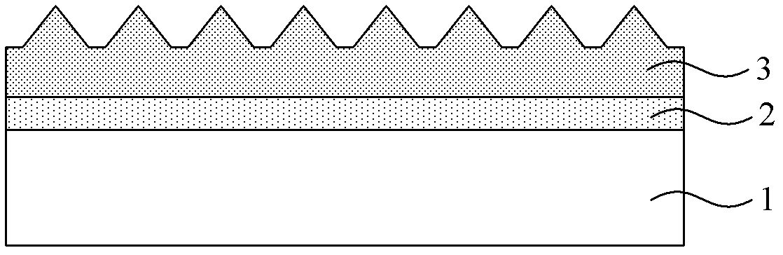
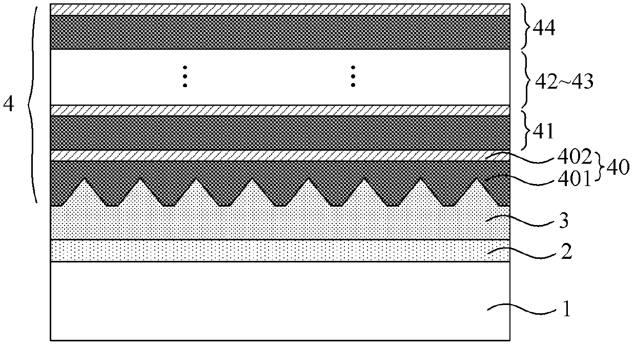
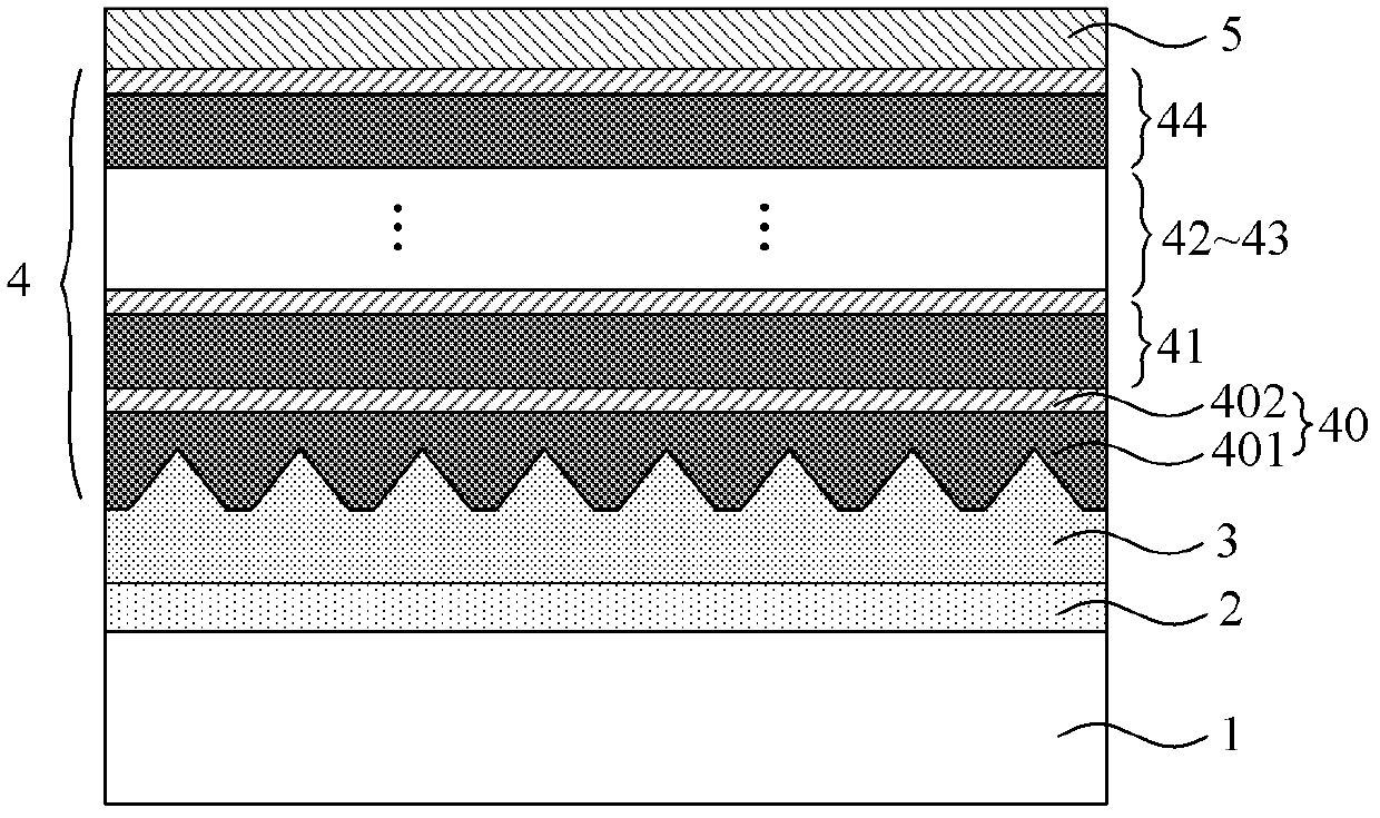
[0036] Such as figure 1 As shown, first perform step 1) to provide a sapphire substrate 1. The substrate is a patterned sapphire substrate (PSS), the substrate pattern is a triangularly arranged cone-shaped high-pack structure, and the bottom of the cone-shaped high-pack The diameter is 2.4μm, the height of the cone is 1.5μm, and the interval between adjacent cones is 0.6μm (duty cycle is 0.8). The metal organic chemical vapor deposition (MOCVD) method is used, when the temperature is 500~600℃ and the pressure When it is 400-600 Torr, epitaxially (two-dimensional growth, layer-by-layer growth, Frank-van der Merwe growth mode) a GaN buffer layer 2 on the sapphire substrate 1, and then when the temperature is 900-1000°C and the pressure is 400 At ~600 Torr, a three-dimensional growth (island g...

Embodiment 2

[0045] The second embodiment adopts basically the same technical solution as the first embodiment, but the difference is: ① When the two superlattices are prepared, although the double-layer film of the superlattice all contains a GaN layer and Al 1-x Ga x N layer, but the GaN layer and the Al 1-x Ga x The upper and lower positions of the N layer are different. In the first embodiment, the double-layer film is the GaN / Al 1-x Ga x N double-layer film, namely each GaN / Al 1-x Ga x Al in N bilayer film 1-x Ga x The N layer is located on the GaN layer, and in the second embodiment, the double-layer film is Al 1-x Ga x N / GaN double-layer film, namely each Al 1-x Ga x The GaN layer in the N / GaN bilayer film is located in Al 1-x Ga x Above the N layer; ②The number of periodic epitaxy of the double-layer film in the superlattice prepared by the two is different. In the first embodiment, the periodic epitaxy of the GaN / Al 1-x Ga x N double-layer film 5 times, and in the second embodiment, th...


PUM


Abstract

The invention provides a method for reducing warping stress of LED epitaxy. The method comprises the steps of forming a GaN buffer layer on a sapphire substrate in an epitaxial mode, then growing a GaN layer on the GaN buffer layer in a three-dimensional mode, and forming a GaN epitaxial wafer which is provided with an island-shaped surface; after cooling is conducted, forming a double-layer thin film on the GaN epitaxial wafer provided with the island-shaped surface in an epitaxial mode, wherein the double-layer thin film comprises the GaN layer and an All-xGaxN layer, and forming double-layer thin films repeatedly in the epitaxial mode so as to form a superlattice on the GaN epitaxial wafer provided with the island-shaped surface; growing the GaN layer on the superlattice in a two-dimensional mode, and finishing preparation of a GaN base layer on the sapphire substrate. A superlattice inserting layer structure is adopted to adjust and release the warping stress between the GaN epitaxial layer growing in the two-dimensional mode and the sapphire substrate, accordingly, the warping degree when a light-emitting layer is grown on the epitaxial wafer is improved, wavelength difference between the central part and the edge part of the epitaxial wafer after the light-emitting layer is grown can be reduced, uniformity of the wavelength of the epitaxial wafer is improved, and accordingly the wave length yield of the epitaxial wafer is improved.

Description

Technical field [0001] The invention relates to the field of LED chip manufacturing, in particular to a method for reducing the epitaxial warping stress of the LED. Background technique [0002] MOCVD (Metal-Organic Chemical Vapor Deposition, metal organic chemical vapor deposition) is a new type of vapor phase epitaxy growth technology developed on the basis of vapor phase epitaxy (VPE) growth. MOCVD uses organic compounds of group III and group II elements and hydrides of group V and VI elements as crystal growth source materials, and conducts vapor phase epitaxy on the substrate by thermal decomposition reaction to grow various groups of III-V and II. -VI compound semiconductors and their multi-element solid solution thin layer single crystal materials. Generally, the crystal growth in MOCVD equipment is under normal pressure or low pressure (10-100 Torr). 2 In the cold wall quartz (stainless steel) reaction chamber, the substrate temperature is 500-1200℃, and the graphite pl...

Claims


Application Information

Patent Timeline
Patent Type & Authority Applications(China)
IPC IPC(8): H01L33/00
Inventor 彭昀鹏潘尧波
Owner EPILIGHT TECH
Why Eureka
Try Eureka