

LED structure capable of reducing working temperature of active area and manufacturing method thereof
A technology of LED structure and working temperature, which is applied in the direction of semiconductor devices, electrical components, circuits, etc., can solve the problems of LED heating, complex energy consumption of cooling means, poor cooling effect, etc., and improve light extraction efficiency , reduce the effective refractive index, and be easy to integrate and prepare
- Summary
- Abstract
- Description
- Claims
- Application Information
AI Technical Summary
Problems solved by technology
Method used
Image

Examples
Embodiment 1
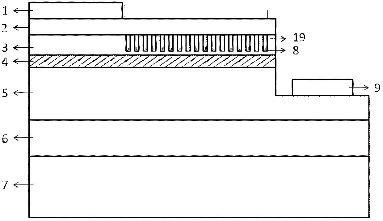
[0056] Example 1. Preparation of LED with 2-inch sapphire substrate with GaN-based electrode structure on the same plane
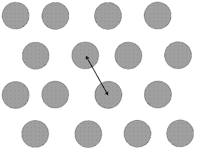
[0057] structured as figure 1 and image 3 As shown, the structure from the bottom to the top of the GaN-based LED with the same plane electrode structure is sapphire substrate layer 7, intrinsic GaN layer 6, n-GaN confinement layer 5, active region light-emitting layer 4, p-GaN confinement layer Layer 3, current spreading layer 2 and p-plane electrode 1; holes 19 are formed on the upper surface of the p-GaN confinement layer 3 to form a hole array, and the holes 19 are arranged six times symmetrically; the period of the holes 19 is 2 μm, The diameter of the hole is 1 μm, and the duty ratio of the hole on the lower surface of the p-GaN confinement layer is 50%; the distance s1 between the bottom edge of the hole 19 and the light-emitting layer 13 in the active region is 30 nm; the bottom of the hole has a thickness of 3 nm silver film.
[0058] The prep...
Embodiment 2
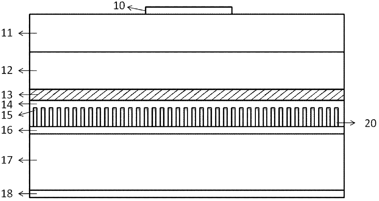
[0064] Embodiment 2. Preparation of LED with GaN-based vertical electrode structure on 2-inch sapphire substrate
[0065] structured as figure 2 and Figure 4 , the LED includes a p-side electrode 18, a sapphire substrate layer 17, a metal reflector 16, a p-GaN confinement layer 14, an active region light-emitting layer 13, an n-GaN confinement layer 12, an intrinsic GaN layer arranged from bottom to top 11 and an n-face electrode 10; holes 20 are formed on the lower surface of the p-GaN confinement layer 14 to form a hole array, and the holes are arranged four times symmetrically; the period of the holes is 10 μm, and the diameter of the holes is 2.5 μm. The duty cycle of the lower surface of the p-GaN confinement layer is 25%; the distance s2 between the bottom of the hole 20 and the light-emitting layer 13 in the active region is 40nm; there is a silver film with a thickness of 5nm at the bottom of the hole 20 .
[0066] The preparation method steps are as follows:
[0...
Embodiment 3
[0072] Example 3. Preparation of an LED with a GaN-based electrode structure on a 2-inch silicon carbide substrate
[0073] structured as figure 1 and Figure 4 , the GaN-based LED with the same-plane electrode structure as described in Embodiment 1, the structure of the GaN-based LED with the same-plane electrode structure from the bottom to the top is a silicon carbide substrate layer 7, an intrinsic GaN layer 6, and n-GaN confinement layer 5, active region light-emitting layer 4, p-GaN confinement layer 3, current spreading layer 2 and p-surface electrode 1; the holes 19 are arranged four times symmetrically; the period of the holes is 20 μm, and the diameter of the holes is 5 μm, so The duty cycle of the hole 19 on the upper surface of the p-GaN confinement layer 3 is 25%; the distance s1 between the bottom of the hole 19 and the light-emitting layer 4 in the active region is 50nm; there is a silver film with a thickness of 10nm at the bottom of the hole.
[0074] The pr...
PUM
| Property | Measurement | Unit |
|---|---|---|
| Diameter | aaaaa | aaaaa |
| Thickness | aaaaa | aaaaa |
| Thickness | aaaaa | aaaaa |
Abstract
Description
Claims
Application Information