InGaN quantum dot epitaxial wafer prepared through substrate with atom step and preparation method thereof
A technology of quantum dots and epitaxial wafers, applied in the field of InGaN quantum dot light-emitting electrical device epitaxial wafers and its preparation, can solve the problems of high In composition InGaN material growth difficulties, luminous efficiency decline, etc., achieve high luminous efficiency, improve overlap The effect of degree and luminosity uniformity
- Summary
- Abstract
- Description
- Claims
- Application Information
AI Technical Summary
Problems solved by technology
Method used
Image

Examples
Embodiment Construction
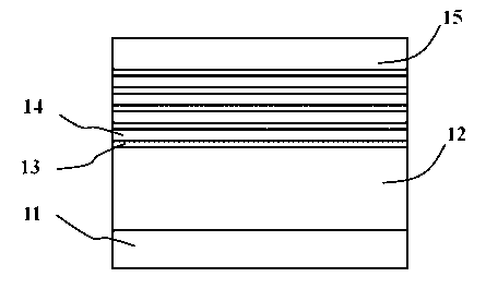
[0025] The invention discloses a substrate with atomic steps to prepare InGaN quantum dot light-emitting device epitaxial wafers. The preparation method includes the following steps:
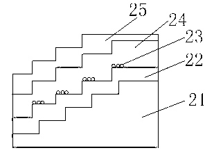
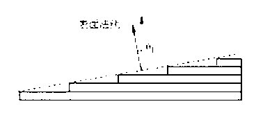
[0026] Get a substrate 21 with atomic steps, this substrate 21 can be sapphire sheet, silicon sheet, silicon carbide sheet, gallium nitride sheet, the bevel angle of substrate surface is θ, for better obtaining 0.05 o o , the chamfer angle refers to the angle between the crystal orientation of the surface of the substrate 21 and the surface normal direction.
[0027] On the substrate 21 , an N-type layer 22 , an active region and a P-type layer 25 are sequentially grown on the substrate by a metal organic chemical vapor deposition (MOCVD) method.
[0028] The active region is n (n≥1) periods of In M Ga 1-M N quantum dot layer 23 and In N Ga 1-N The light-emitting active region formed by the N barrier layer 24 (0N). The atomic steps on the surface of the substrate 21 will be followed in the ...
PUM
 Abstract
Description
Claims
Application Information
 - R&D
- Intellectual Property
- Life Sciences
- Materials
- Tech Scout
- Unparalleled Data Quality
- Higher Quality Content
- 60% Fewer Hallucinations
Browse by: Latest US Patents, China's latest patents, Technical Efficacy Thesaurus, Application Domain, Technology Topic, Popular Technical Reports.
© 2025 PatSnap. All rights reserved.Legal|Privacy policy|Modern Slavery Act Transparency Statement|Sitemap|About US| Contact US: help@patsnap.com