Semiconductor power module package structure and preparation method thereof

A power module and packaging structure technology, which is applied in semiconductor/solid-state device manufacturing, semiconductor devices, semiconductor/solid-state device components, etc., can solve the problems of inflexible combination, insecurity, and electrification of supporting platforms, and achieve physical volume reduction, The effect of improving the service life and expanding the application field

Active Publication Date: 2013-09-18
SHENZHEN STS MICROELECTRONICS
View PDF4 Cites 18 Cited by
  • Summary
  • Abstract
  • Description
  • Claims
  • Application Information

AI Technical Summary

Problems solved by technology

[0005] ①. The support platform of traditional semiconductor power devices is generally made of pure copper and is integrated. It is impossible to design complex circuits on its surface, and it is also impossible to integrate more chips.
If you want to integrate multiple power devices, you can only package a single chip, such as IGBT, and then realize it through an external auxiliary circuit, which will form a huge circuit structure volume
[0006] ②. The heat sink is the G pole of the chip. When the power semiconductor module is working, the support platform (heat sink) is charged and unsafe.
[0007] ③, the expansion coefficient of copper is 17×10 -6 / ℃, and the expansion coefficient of silicon (the main component of the chip) is 3.2×10 -6 / °C ratio, the difference is large, and the thermal expansion during use is likely to cause delamination, which affects the life of the power semiconductor module
[0008] ④. Because the heat sink of the power semiconductor module is produced together with the lead frame, once it is finished, it will be finalized. One type of heat sink is bound to one type of lead frame, which cannot be combined flexibly according to the demand, which increases the difficulty of design and production

Method used


Image

  • Semiconductor power module package structure and preparation method thereof
  • Semiconductor power module package structure and preparation method thereof
  • Semiconductor power module package structure and preparation method thereof

Examples


Embodiment Construction

[0040] Attached below Figure 1-4 , the specific embodiment of the present invention will be further described in detail.

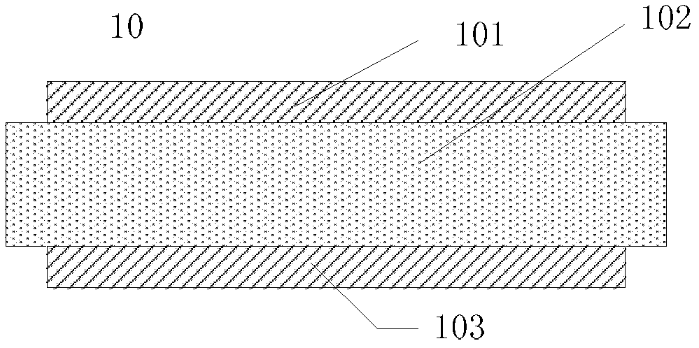
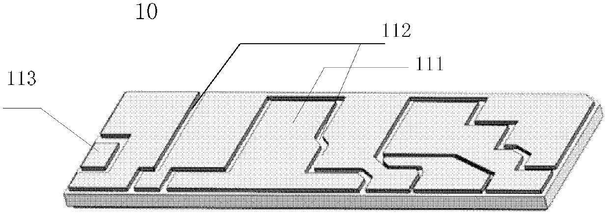
[0041]The power semiconductor module packaging structure based on the copper-clad ceramic substrate provided by the present invention is suitable for any power semiconductor module packaging structure that includes multiple power drive chips and frequency conversion control chips integrated in a compact physical volume and small external dimensions . Before introducing the present invention, first briefly introduce the copper-clad ceramic substrate.

[0042] Copper-clad ceramic substrate is made by directly bonding copper foil to the upper and lower surfaces of the ceramic substrate at high temperature. It has electrical insulation performance, high thermal conductivity and high mechanical strength. It not only has excellent solderability and High adhesion strength, and the coefficient of thermal expansion is close to that of silicon, it is an ideal sub...


PUM


Abstract

A semiconductor power module package structure comprises a dual in-line type package shell, a copper-coated ceramic substrate, at least one power drive chip, a printed circuit board and a lead frame. The top layer of the copper-coated ceramic substrate includes a first lead pad, an insulating groove and a welding platform. The at least one power drive chip is mounted on the welding platform in the top layer of the copper-coated ceramic substrate and a pin of the power drive chip is connected with the first lead pad. An auxiliary circuit and a second lead pad are arranged on the printed circuit board, at least one frequency conversion control chip is mounted on the printed circuit board, and a pin of the frequency conversion control chip is connected with the corresponding second lead pad. The lead frame includes a first-side connecting pin used for power drive signal transmission and a second-side connecting pin used for frequency conversion control signal transmission, the first-side connecting pin is respectively connected with the first lead pad and the second lead pad, and the second-side connecting pin is connected with the corresponding second lead pad. A power drive circuit and a frequency conversion control circuit are packaged together in the semiconductor power module package structure, and the semiconductor power module package structure is small in size, convenient for users to use and wider in application occasion.

Description

technical field [0001] The present invention relates to semiconductor chip packaging technology, more specifically, to a semiconductor power module packaging structure and a preparation method thereof. Background technique [0002] Power semiconductor modules are mainly used in power conversion applications, such as control and monitoring equipment, motor drives, and power transmission and transformation. The power driving circuit generally includes an insulated gate bipolar transistor (Insulated Gate Bipolar Transistor, IGBT for short), a metal-oxide-semiconductor field-effect transistor (Metal-Oxide-Semiconductor Field-Effect Transistor, MOSFET for short), a thyristor, and a power diode. [0003] With the increase of the performance of power semiconductor modules, the number of chips contained in intelligent power modules is increasing sharply, which puts forward higher requirements for large-scale integrated circuits. Evaluating the performance of power semiconductor mod...

Claims


Application Information

Patent Timeline
Patent Type & Authority Applications(China)
IPC IPC(8): H01L23/367H01L23/373H01L23/00H01L21/50
CPCH01L2924/0002H01L2924/00
Inventor 孙复生巴利生郑慧灵
Owner SHENZHEN STS MICROELECTRONICS
Why Eureka
Try Eureka