Laser stripping film LED (Light-Emitting Diode) and preparation method thereof

A laser lift-off and thin-film technology, which is applied in the direction of semiconductor devices, electrical components, circuits, etc., can solve the problems of absolute efficiency enhancement that has not been reported, and achieve the goal of increasing radiation recombination efficiency and light extraction efficiency, simplifying the manufacturing process, and reducing the difficulty of preparation Effect

Active Publication Date: 2013-09-18
PEKING UNIV
View PDF5 Cites 29 Cited by
  • Summary
  • Abstract
  • Description
  • Claims
  • Application Information

AI Technical Summary

Problems solved by technology

Yang Zhizhong and others only realized the SP-enhanced LED structure on the surface of an ordinary chip, and there is no report on the absolute efficiency enhancement under large injection
At the same time, there is no report on the application of plasmonic structures in thin-film LEDs so far.

Method used


Image

  • Laser stripping film LED (Light-Emitting Diode) and preparation method thereof
  • Laser stripping film LED (Light-Emitting Diode) and preparation method thereof
  • Laser stripping film LED (Light-Emitting Diode) and preparation method thereof

Examples


Embodiment Construction

[0052] The present invention will be further described through the embodiments below in conjunction with the accompanying drawings.

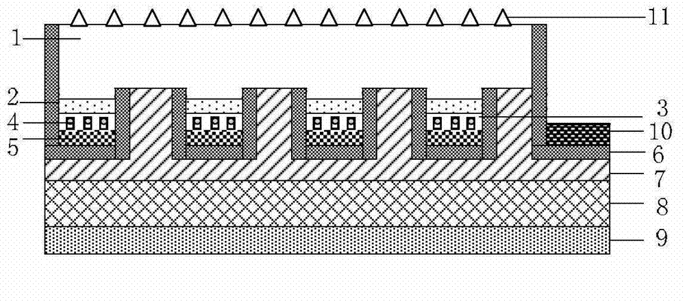
[0053] Such as figure 1 As shown, the chip unit of the laser lift-off film LED of the present invention includes: a chip part and a substrate; the chip part includes: an n-type layer 1, which has periodic n-type blind holes corresponding to the protrusions of the n-electrode on the n-type layer , the quantum well 2 between the periodic n-type blind holes on the n-type layer, the p-type layer 3 on the quantum well, the periodic metal nanostructure 4 embedded on the p-type layer, and the p-type layer The p-electrode 5 on the top, the insulating layer 6 on the p-electrode and the sidewall of the n-type blind hole, the n-electrode 7 on the insulating layer, the n-electrode has periodic protrusions, and the periodic protrusions extend into the n-type layer Inside; the substrate includes an electrically and thermally conductive substrate 8 and an n-e...


PUM

PropertyMeasurementUnit
sizeaaaaaaaaaa
sizeaaaaaaaaaa
sizeaaaaaaaaaa

Abstract

The invention discloses a laser stripping film LED (Light-Emitting Diode) and a preparation method thereof. A chip unit of the laser stripping film LED comprises a type n layer, a quantum well, a type p layer, a periodical metal nanometer structure, an electrode p, an insulating layer and an electrode n, wherein the type p layer is formed on the quantum well; the periodical metal nanometer structure is embedded into the type p layer; the abovementioned structures inversely cover on a substrate; and a bonding pad p is arranged at one corner of a chip. According to the laser stripping film LED, the coupling resonance functions of surface plasmons and a quantum well structure are utilized, so that the radiation compounding efficiency and light-emitting efficiency of the LED are increased greatly under bulk injection, and meanwhile, certain effects are achieved on green-yellow light and ultraviolet light LEDs with low light-emitting efficiency; laser scribing and corroding methods are adopted for partitioning the chip unit, so that the warping of an epitaxial wafer is reduced, and the processing difficulty and cost are lowered; and specific to the bonding pad p, a protection layer and silver layer evaporation process is adopted, so that the manufacturing process of the bonding pad p is simplified, and the process cost is lowered; and a hot phosphoric acid coarsening method is adopted, so that the process cost is lowered, and the light-emitting efficiency of the LED is increased.

Description

technical field [0001] The invention relates to a semiconductor chip preparation technology, in particular to a laser stripping film LED and a preparation method thereof. Background technique [0002] Thin-film light-emitting diode (Light Emitting Diode) LED chips have been used by many LED manufacturers since they were proposed by Schnitzer et al. in 1993 (Appl. Phys. Lett., 63(16), 2174(1993)). Compared with traditional LED chips, it has good heat dissipation, uniform current expansion, and excellent light emission structure, which is very suitable for the application of high-efficiency and high-power LEDs, and is currently a high-end product of LEDs. In particular, the recently published TFFC chips of LumiLEDs and UX:3 chips of Osram overcome the difficulties of preparing electrodes and bonding wires on thin films, and show good application prospects. However, the flip-chip, primer or flip-chip eutectic soldering process used by LumiLEDs has great process difficulty and ...

Claims


Application Information

Patent Timeline
Patent Type & Authority Applications(China)
IPC IPC(8): H01L33/20H01L33/00
Inventor 陈志忠焦倩倩姜爽付星星姜显哲马健张国义
Owner PEKING UNIV
Why Eureka
Try Eureka