Preparation method and application of self-assembled nanometer metal or semiconductor particle doped graphene microsheets
A graphene microchip and nano-metal technology, applied in the direction of graphene, nano-carbon, etc., can solve problems such as difficult to use, poor controllability, complicated and heavy experimental steps, etc., to achieve selectivity and diversity optimization, strong The effect of the function
- Summary
- Abstract
- Description
- Claims
- Application Information
AI Technical Summary
Problems solved by technology
Method used
Image

Examples
Embodiment 1
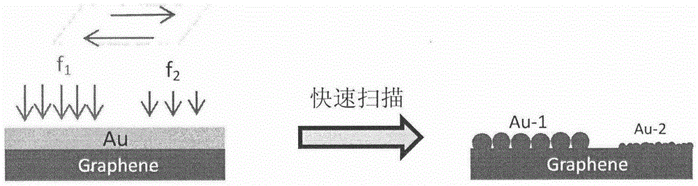
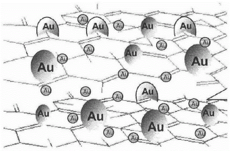
[0025] 1. Paste the graphene oxide paper (thickness 13um, source: Changzhou Sixth Element Co., Ltd.) on the surface of the clean silicon wafer, and place it on the substrate stage in the vacuum evaporation coating chamber. Put 0.15g of gold wire in the molybdenum boat of the evaporation source. Cover the bell jar, turn on the mechanical pump, backing valve and molecular pump, and wait for the vacuum gauge to show that the vacuum in the chamber is pumped to 10 -4 At Pa, turn on the evaporation power supply and the film thickness tester; adjust the power supply current to 22 amperes, the molybdenum boat starts to turn red, and the gold wire melts and sprays and deposits toward the graphene oxide paper sample (deposition rate is about 1-2nm / s). When the thickness of the deposited gold film is detected to increase to 60nm with a film thickness meter (the surface of the sample appears light golden at this time), the evaporation power is turned off. Air is introduced into the coati...
Embodiment 2
[0030] 1. Paste the graphene oxide paper (thickness 13um, source: Changzhou Sixth Element Co., Ltd.) on the surface of the clean silicon wafer, and place it on the substrate stage in the vacuum evaporation coating chamber. 0.12g of silver wire was placed in the molybdenum boat of the evaporation source. Cover the bell jar, turn on the mechanical pump, backing valve and molecular pump, and wait for the vacuum gauge to show that the vacuum in the chamber is pumped to ~10 -4 When Pa, turn on the evaporation power supply and the film thickness tester; adjust the power supply current to 16 amperes, the molybdenum boat starts to turn red, and the silver wire melts and sprays and deposits toward the graphene oxide paper sample (the deposition rate is about 1-2nm / s). When the thickness of the deposited silver film is detected by a film thickness meter to increase to 60nm (at this time, the surface of the sample appears light silver), turn off the evaporation power supply. Air is intr...
Embodiment 3
[0035] 1. Paste the graphene oxide paper (thickness 13um, source: Changzhou Sixth Element Co., Ltd.) on the surface of the clean silicon wafer, and place it on the substrate stage in the vacuum evaporation coating chamber. A 0.12 g silicon oxide wafer was placed in a tungsten boat in the evaporation source. Cover the bell jar, turn on the mechanical pump, backing valve and molecular pump, and wait for the vacuum gauge to show that the vacuum in the chamber is pumped to ~10 -4 At Pa, turn on the evaporation power supply and the film thickness tester; adjust the power supply current to 45 amperes, the tungsten boat starts to turn red, the silicon oxide sheet melts and sprays and deposits toward the graphene oxide paper sample (deposition rate is about 1-2nm / s). When the thickness of the deposited silicon oxide film is detected by a film thickness meter to 60nm, turn off the evaporation power supply. Air is introduced into the coating chamber to normal pressure, and the bell jar...
PUM
| Property | Measurement | Unit |
|---|---|---|
| thickness | aaaaa | aaaaa |
Abstract
Description
Claims
Application Information
 - R&D
- Intellectual Property
- Life Sciences
- Materials
- Tech Scout
- Unparalleled Data Quality
- Higher Quality Content
- 60% Fewer Hallucinations
Browse by: Latest US Patents, China's latest patents, Technical Efficacy Thesaurus, Application Domain, Technology Topic, Popular Technical Reports.
© 2025 PatSnap. All rights reserved.Legal|Privacy policy|Modern Slavery Act Transparency Statement|Sitemap|About US| Contact US: help@patsnap.com