Molecular Beam Epitaxy Growth Method of Gaas-Based Nanowires Regulated by Bi Elements

A technology of molecular beam epitaxy and crystal structure, which is applied in the directions of crystal growth, single crystal growth, single crystal growth, etc., can solve the problems affecting the uniformity of photoelectric device performance and unfavorable growth of nanowires with uniform length and thickness, so as to achieve excellent materials and high reliability. The effect of growth control

Inactive Publication Date: 2015-07-29
SHANGHAI INST OF TECHNICAL PHYSICS - CHINESE ACAD OF SCI
View PDF0 Cites 0 Cited by
  • Summary
  • Abstract
  • Description
  • Claims
  • Application Information

AI Technical Summary

Problems solved by technology

[0003] However, the crystal structure of GaAs-based nanowires grown by the gas-liquid-solid growth method in MBE mainly exhibits a wurtzite structure; although GaAs-based nanowires with a sphalerite structure can be grown by adjusting the growth process parameters, at this time The growth process conditions are already at the edge of the GaAs-based nanowire growth process window, which is not conducive to the growth of upright nanowires with uniform length and thickness, which will seriously affect the performance uniformity of the prepared GaAs-based nanowire optoelectronic devices

Method used


Image

  • Molecular Beam Epitaxy Growth Method of Gaas-Based Nanowires Regulated by Bi Elements
  • Molecular Beam Epitaxy Growth Method of Gaas-Based Nanowires Regulated by Bi Elements

Examples


Embodiment 1

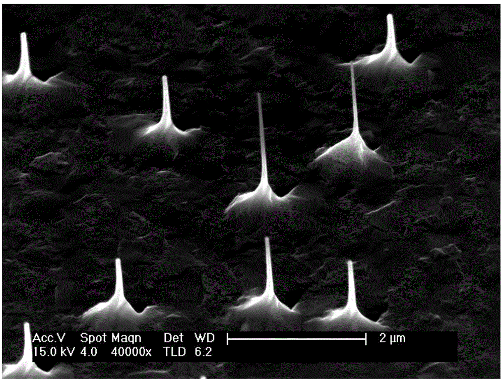
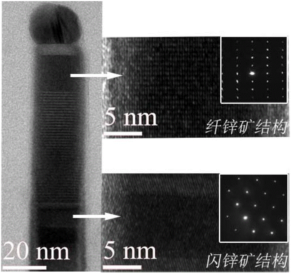
[0017] In this example, the temperature of the storage furnace of the As evaporation source is controlled at 180°C, the temperature of the Ga evaporation source is controlled at 950°C, and the temperature of the Bi evaporation source is controlled at 480°C, so that x=40%. The GaAs(111)B substrate was loaded into the MBE growth chamber, and the growth temperature was controlled at 420°C. After growing GaAs nanowires for 10 minutes, under the condition that the growth conditions remained unchanged, the Bi evaporation source baffle was opened, and Bi element was introduced to reduce the ionic type of GaAs, thereby promoting the formation of zinc blende structure GaAs nanowires, and the growth After cooling the substrate and each evaporation source, the sample is introduced into the MBE pretreatment chamber to take out the GaAs nanowires with coexistence of wurtzite structure and sphalerite structure. High-resolution transmission electron microscopy and selected area electron diff...

Embodiment 2

[0019] In this example, the temperature of the storage furnace of the As evaporation source is controlled at 180°C, the temperature of the Ga evaporation source is controlled at 950°C, and the temperature of the Bi evaporation source is controlled at 500°C, so that x=66%. The GaAs(111)B substrate was loaded into the MBE growth chamber, and the growth temperature was controlled at 420°C. After growing GaAs nanowires for 10 minutes, under the condition that the growth conditions remained unchanged, the Bi evaporation source baffle was opened, and Bi element was introduced to reduce the ionic type of GaAs, thereby promoting the formation of zinc blende structure GaAs nanowires, and the growth After cooling the substrate and each evaporation source, the sample is introduced into the MBE pretreatment chamber to take out the GaAs nanowires with coexistence of wurtzite structure and sphalerite structure. High-resolution transmission electron microscopy and selected area electron diff...

Embodiment 3

[0021] In this example, the temperature of the storage furnace of the As evaporation source is controlled at 180°C, the temperature of the Ga evaporation source is controlled at 940°C, and the temperature of the Bi evaporation source is controlled at 500°C, so that x=50%. The GaAs(111)B substrate was loaded into the MBE growth chamber, and the growth temperature was controlled at 420°C. After growing GaAs nanowires for 10 minutes, under the condition that the growth conditions remained unchanged, the Bi evaporation source baffle was opened, and Bi element was introduced to reduce the ionic type of GaAs, thereby promoting the formation of zinc blende structure GaAs nanowires, and the growth After cooling the substrate and each evaporation source, the sample is introduced into the MBE pretreatment chamber to take out the GaAs nanowires with coexistence of wurtzite structure and sphalerite structure. High-resolution transmission electron microscopy and selected area electron diff...


PUM

PropertyMeasurementUnit
thicknessaaaaaaaaaa

Abstract

The invention discloses a molecular beam epitaxial (MBE) growth method of a Bi element regulated and controlled GaAs-based nanowire crystal structure. A Bi element is introduced as an activating agent during the growing process of nanowires in an MBE growth chamber, the ionicity of GaAs is reduced, and the formation of a nanowire zinc blende structure is promoted. The method is characterized in that the Bi evaporator source temperature is regulated during the process of nanowire growth according to the beam equivalent partial pressure of a Ga element so as to control the beam equivalent partial pressure of the Bi element and to ensure that the ratio of the beam equivalent partial pressure of the Bi element to that of the Ga element is x, and the value of x can influence the regulating and controlling ability of the Bi element to the nanowire crystal structure and influence the feature and the phase structure purity of the nanowires. The method has the benefits that the growth of the GaAs-bases nanowires with the zinc blende crystal structure can be easily realized without changing the growth process conditions of MBE, and thus the method is beneficial to the controlled growth of the GaAs-based nanowires with the wurtzite and zinc blende structure and the formation of a homogeneous heterophase heterogeneous structure of the nanowires, and provides an excellent material for preparing nanoscale photoelectronic devices.

Description

technical field [0001] The invention belongs to the technical field of new nanometer material growth, and in particular relates to a molecular beam epitaxy growth method in which Bi element regulates the crystal structure of GaAs-based nanowires. It grows GaAs-based nanowires with coexistence of wurtzite structure and sphalerite structure by introducing Bi element in the MBE growth chamber under the condition of constant growth conditions, ie growth temperature, V-III beam ratio, etc. technical background [0002] In recent years, one-dimensional semiconductor nanowires have become a new generation of materials for the preparation of nanoscale optoelectronic devices due to their excellent performance in electrical, optical, mechanical and thermal aspects. The III-V group semiconductor represented by gallium arsenide GaAs has the characteristics of direct band gap, high electron mobility, and small effective mass, and the optoelectronic device based on the III-V group semicon...

Claims


Application Information

Patent Timeline
Patent Type & Authority Patents(China)
IPC IPC(8): C30B29/62C30B29/42C30B23/02
Inventor 陈平平卢振宇陆卫石遂兴周孝好
Owner SHANGHAI INST OF TECHNICAL PHYSICS - CHINESE ACAD OF SCI
Why Eureka
Try Eureka