Black phosphorus film as well as preparation method and application thereof

A black phosphorus and thin film technology, applied in the field of two-dimensional materials, can solve the problems of difficulty in realizing large-scale preparation and industrialization of black phosphorus materials and devices, inability to control the thickness and size of black phosphorus films, and difficulty in controlling the size and thickness of black phosphorus. , to achieve the effect of convenient large-scale research and development and application, low price of raw materials, and good photoelectric performance

Inactive Publication Date: 2020-06-26
SUZHOU INST OF NANO TECH & NANO BIONICS CHINESE ACEDEMY OF SCI
View PDF3 Cites 6 Cited by
  • Summary
  • Abstract
  • Description
  • Claims
  • Application Information

AI Technical Summary

Problems solved by technology

The mechanical exfoliation method is to separate the black phosphorus nanosheets from the black phosphorus crystal by applying mechanical force (friction force, pulling force, etc.) to the black phosphorus block. This method is simple and easy, but the thickness and size of the black phosphorus film cannot be controlled. , low preparation efficiency [L.Li, et.al, Nat.Nanotechnol.2014,9,372.]
The liquid phase dispersion method is to disperse black phosphorus crystals by means of ultrasound, centrifugation, etc. to prepare black phosphorus nanosheets [P.Yasaei, et.al, Adv. Mater., 2015, 27:1887-1892.] [D. et al.Nat.Commun.,2015,6:8563], this method also has problems such as difficulty in controlling the size and thickness of black phosphorus
Plasma etching realizes the thinning of black phosphorus through the reaction of plasma groups and phosphorus atoms to generate volatile products [Jiajie Pei, et al. Nat. Commun., 2016, 7: 10450.], but the physical Bombardment will cause damage to black phosphorus, and residual chemical impurities will introduce pollution and affect the performance of black phosphorus
The above methods are difficult to achieve large-scale preparation and industrialization of black phosphorus materials and devices

Method used


Image

  • Black phosphorus film as well as preparation method and application thereof
  • Black phosphorus film as well as preparation method and application thereof
  • Black phosphorus film as well as preparation method and application thereof

Examples


preparation example Construction

[0044] The invention provides a method for preparing a black phosphorus film, comprising:

[0045] S100: placing a growth substrate, a phosphorus-containing precursor, and a mineralizer in a vacuum-tight reaction chamber, wherein the growth substrate and the phosphorus-containing precursor are placed in different regions of the vacuum-tight reaction chamber ;

[0046] S200: heating the reaction chamber and keeping it warm, causing the mineralizer to react with the phosphorus-containing gas partially derived from the phosphorus-containing precursor, and forming an induced nucleation point for inducing black phosphorus crystallization on the growth substrate or Induced nucleation layer;

[0047] S300: Lowering the temperature of the reaction chamber, depositing the phosphorus-containing gas on the growth substrate, and epitaxially growing the black phosphorus film under the induction of the induced nucleation point or the induced nucleation layer.

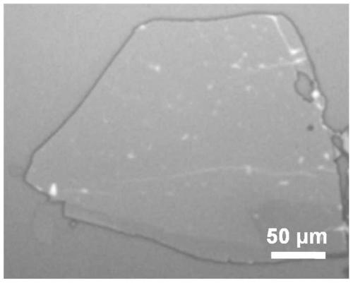
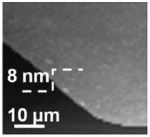
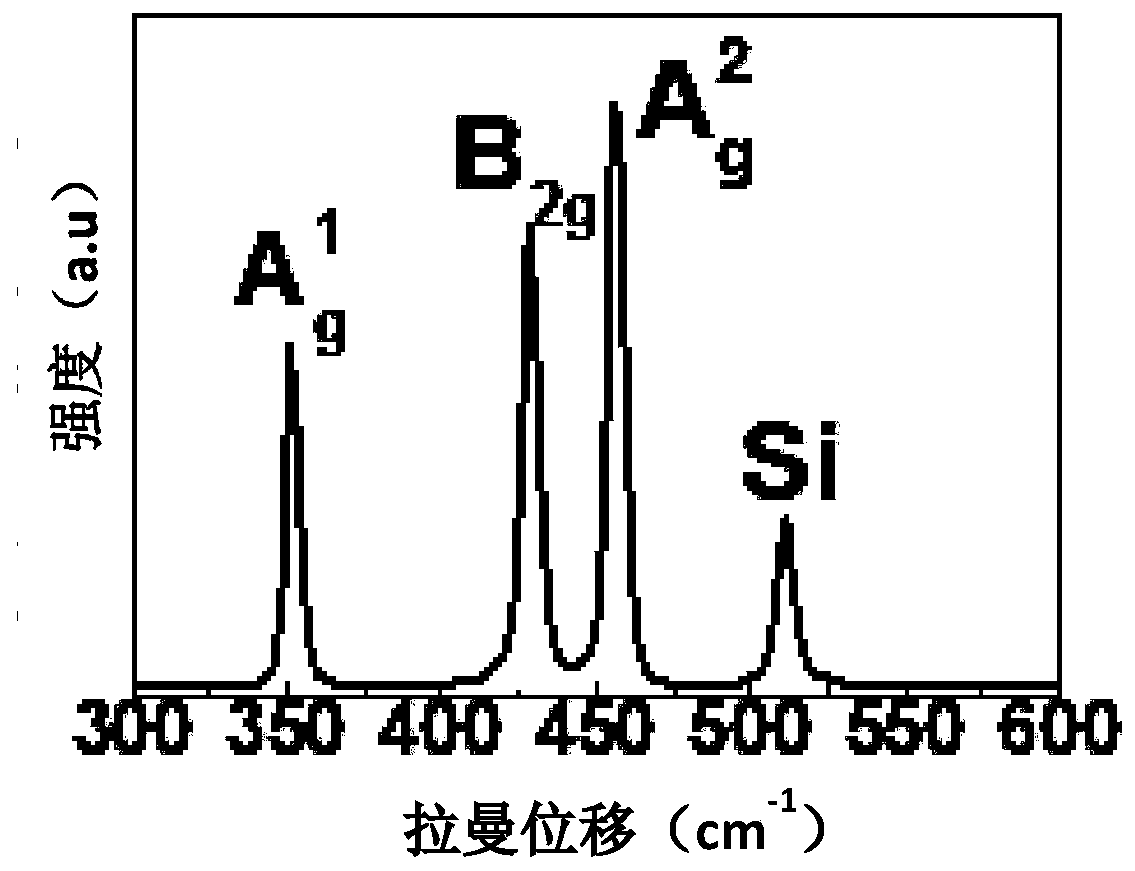
[0048] In the embodiment of...

Embodiment 1

[0096] This embodiment discloses a method for preparing a black phosphorus thin film, which specifically includes:

[0097] (1) Formation of induced nucleation sites or induced nucleation layers

[0098] a) Provide multiple silicon dioxide growth substrates, red phosphorus and mineralizers, the mineralizers include tin iodide, tin and gold, wherein the gold is uniformly arranged on the silicon dioxide growth substrates A layer of gold film, the thickness of the gold film is 5-180nm;

[0099] b) placing the tin iodide, tin and red phosphorus at the low-temperature end in the vacuum-sealed reaction chamber, and placing the growth substrate at the high-temperature end in the vacuum-sealed reaction chamber, wherein multiple growth substrates are stacked and arranged at intervals;

[0100] c) heating the reaction chamber to 750°C at a rate of 10°C / min, and keeping it warm for 1h;

[0101] Wherein, the mass ratio of the tin iodide, tin and red phosphorus is 1:(2-10):(10-100).

[...

Embodiment 2

[0112] This embodiment discloses a method for preparing a black phosphorus thin film, which specifically includes:

[0113] (1) Formation of induced nucleation sites or induced nucleation layers

[0114] a) Provide multiple silicon dioxide growth substrates, white phosphorus and mineralizers, the mineralizers include tin iodide, tin and gold, wherein the gold is a layer evenly arranged on the silicon dioxide growth substrates A gold film, the thickness of the gold film is 5-180nm;

[0115] b) placing the tin iodide, tin and red phosphorus at the low-temperature end in the vacuum-sealed reaction chamber, and placing the growth substrate at the high-temperature end in the vacuum-sealed reaction chamber, wherein multiple growth substrates are stacked and arranged at intervals;

[0116] c) heating the reaction chamber to 650°C at a rate of 20°C / min, and keeping it warm for 2.5h;

[0117] Wherein, the mass ratio of the tin iodide, tin and white phosphorus is 1:(2-20):(10-200).

...


PUM

PropertyMeasurementUnit
thicknessaaaaaaaaaa
thicknessaaaaaaaaaa
thicknessaaaaaaaaaa

Abstract

The invention relates to the technical field of two-dimensional materials, in particular to a preparation method of a black phosphorus film. The preparation method is characterized in that a growth substrate, a phosphorus-containing precursor and a mineralizer are placed in a vacuum closed reaction chamber, wherein the growth substrate and the phosphorus-containing precursor are placed in different areas in the vacuum closed reaction chamber; the reaction chamber is heated and subjected to heat preservation, so that the mineralizer reacts with part of phosphorus-containing gas from the phosphorus-containing precursor, and an induced nucleating point or an induced nucleating layer for inducing black phosphorus crystallization is formed on the growth substrate; and the temperature of the reaction chamber is reduced, the phosphorus-containing gas is deposited on the growth substrate and epitaxially grows under the induction of the induction nucleating point or the induction nucleating layer to form the black phosphorus film. The black phosphorus film has high quality, high crystallinity and strong repeatability, is suitable for large-area and batch production of the black phosphorus film, and meets the industrial requirements in practical application.

Description

technical field [0001] The invention relates to the technical field of two-dimensional materials, in particular to a black phosphorus film, its preparation method and application. Background technique [0002] In recent years, two-dimensional materials have attracted widespread attention and research boom in academia and industry due to their excellent properties. Among them, graphene has excellent mechanical, optical, thermal and electrical properties, so graphene has great application potential in many fields such as electronics, sensing, energy storage, optoelectronics, and semiconductors. However, graphene also has some shortcomings. Since the band gap of graphene is zero, its application in fields such as semiconductor logic devices and photodetection is limited. To address this issue, scientists have developed other 2D materials such as transition metal dichalcogenides (TMDCs), including MoS 2 、WSe 2 、WS 2 Wait. Two-dimensional TMDCs materials have a bandgap width...

Claims


Application Information

Patent Timeline
Patent Type & Authority Applications(China)
IPC IPC(8): C23C16/28C30B25/18C30B29/02
CPCC23C16/28C30B25/183C30B29/02
Inventor 张凯徐轶君史鑫尧
Owner SUZHOU INST OF NANO TECH & NANO BIONICS CHINESE ACEDEMY OF SCI
Why Eureka
Try Eureka