Preparation method of metallization layer on surface of AIN film

A metallized layer and film surface technology, applied in metal material coating process, coating, ion implantation plating, etc., can solve the problems of weak bonding between the substrate and the metal film, poor structural stability, and difficult sintering of AlN substrates. Achieve the effects of low price, stable structure and low manufacturing cost

Inactive Publication Date: 2013-10-02
SHANGHAI UNIV
View PDF5 Cites 8 Cited by
  • Summary
  • Abstract
  • Description
  • Claims
  • Application Information

AI Technical Summary

Problems solved by technology

[0012] The preparation technology of the metallized layer on the surface of the AlN ceramic substrate is limited by the difficulty of sintering the large-area AlN substrate, the weak bonding force between the substrate and the metal film, and poor structural stability, making it difficult for AlN materials to be used in the microelectronics industry. Technical Barriers to Widespread Adoption

Method used


Image

  • Preparation method of metallization layer on surface of AIN film
  • Preparation method of metallization layer on surface of AIN film
  • Preparation method of metallization layer on surface of AIN film

Examples


Embodiment

[0036] The specific preparation process and steps in this embodiment are as follows:

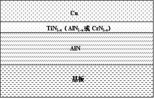
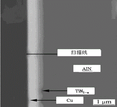
[0037] (1) AlN film is grown on Si substrate by magnetron sputtering method. Process parameters: the target material is Al target, the power is 280W, the gas flow rate of argon and nitrogen is 9sccm, and the sputtering time is 120min. The thickness of the grown AlN film is about 2 μm, and it grows preferentially along the c-axis (0001) direction.

[0038] (2) Growth of TiN on AlN film by magnetron sputtering 1-x (x=0-1) film. Process parameters: The target material is Ti target, the power is 100W, the flow rate of argon gas is 15 sccm, the flow rate of nitrogen gas is gradually reduced from 9 sccm to 0, and the sputtering time is 30 min. Growth of TiN with good orientation 1-x film, the thickness of the film is about 300nm.

[0039] (3) In Si / AlN / TiN 1-x Continue to grow Cu film on the composite film by magnetron sputtering. Process parameters: The target material is pure Cu target, t...


PUM


Abstract

The invention relates to a preparation method of a metallization layer on the surface of an AIN film, which is applied to the fields of circuit substrates and encapsulation in the microelectronics industry. The method comprises the following steps of: in a vacuum environment and under certain growth temperature condition, growing an AIN film with the required thickness on the surface of a substrate by a magnetron sputtering method; growing a TiN(1-x), AlN(1-x) or CrN(1-x) (x=0-1) gradient film on the surface of the AIN film in a sputtering manner, wherein x gradually transits from 0 to 1, namely a nitrogen-rich phase gradually transits to a pure-metal phase; and finally, growing a pure Cu film in a sputtering manner at a proper temperature. Moreover, Cu can be electroplated by an electroplating process according to the use requirement on thickness of the Cu film so that the Cu film is thickened, and proper annealing treatment is performed after each step of film growth process, so as to improve the binding force between the film layers. The film obtained by the method has the advantages of high purity and strong adhesion, and the welding strength and reliability in the encapsulation process are guaranteed.

Description

technical field [0001] The invention relates to a method for preparing a metallized layer on the surface of an AlN film. The method can be used to form a surface metallized layer on the surface of the AlN film and various metals, and is especially suitable for the field of circuit substrates and packaging in the microelectronics industry. Background technique [0002] In recent years, with the development of large-scale integrated circuits and electronic equipment in the direction of high frequency, high power, and ultra-high integration, the demand for high-performance, high-density circuits in various applications is increasing. However, the continuous improvement of circuit density and function leads to continuous increase of circuit power and heat generation per unit time, so that the operating temperature of the circuit is also continuously increased. In order to prevent circuit components from being damaged due to heat accumulation and thermal cycling, this puts forwar...

Claims


Application Information

Patent Timeline
Patent Type & Authority Applications(China)
IPC IPC(8): C23C14/06C23C14/35
Inventor 陈益钢刘震张斌朱涛陈银儿
Owner SHANGHAI UNIV
Why Eureka
Try Eureka