Preparation method of InN (indium nitride) thin film through low-temperature deposition on self-supporting diamond thick film by ECR-PEMOCVD (electron cyclotron resonance-plasma enhanced metal organic chemical vapor deposition)

A diamond thick film, self-supporting technology, applied in metal material coating process, gaseous chemical plating, coating, etc., can solve the problems of high decomposition temperature of nitrogen source, lack of substrate material, low growth temperature, etc., and achieve cost Low, excellent heat resistance, high thermal conductivity effect

A diamond thick film, self-supporting technology, applied in metal material coating process, gaseous chemical plating, coating, etc., can solve the problems of high decomposition temperature of nitrogen source, lack of substrate material, low growth temperature, etc., and achieve cost Low, excellent heat resistance, high thermal conductivity effect

CN103334089AActive Publication Date: 2013-10-02SHENYANG JIAYUE ELECTRIC POWER TECH CO LTD

Image

  • Preparation method of InN (indium nitride) thin film through low-temperature deposition on self-supporting diamond thick film by ECR-PEMOCVD (electron cyclotron resonance-plasma enhanced metal organic chemical vapor deposition)
  • Preparation method of InN (indium nitride) thin film through low-temperature deposition on self-supporting diamond thick film by ECR-PEMOCVD (electron cyclotron resonance-plasma enhanced metal organic chemical vapor deposition)
  • Preparation method of InN (indium nitride) thin film through low-temperature deposition on self-supporting diamond thick film by ECR-PEMOCVD (electron cyclotron resonance-plasma enhanced metal organic chemical vapor deposition)

Examples


Embodiment 1

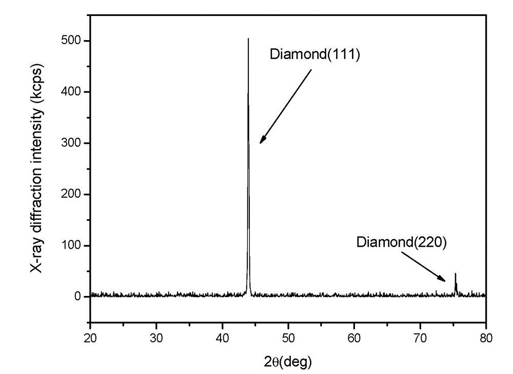
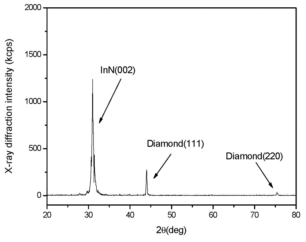
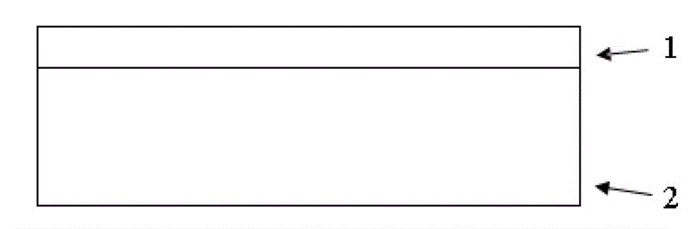
[0036] The free-standing diamond substrate was cleaned with acetone, ethanol and deionized water with ultrasonic in turn, dried with nitrogen and sent to the reaction chamber; the reaction chamber was evacuated to 9.0×10 -4 Pa, heat the substrate to 200℃, and pass trimethyl indium (TMIn) and nitrogen (N 2 ), where TMIn and N 2 The reaction source flow ratio is controlled at 1:100, controlled by the mass flowmeter, the flow parameters are 1 sccm and 100 sccm respectively; the total pressure of the control gas is 1.0Pa; the electron cyclotron resonance frequency is 650W, the reaction is 30min, and the self-supporting diamond thickness is obtained InN photoelectric film on the film substrate.

[0037] After the experiment, Hall test equipment was used to test and analyze the mobility and carrier concentration of the film. The results are shown in Table 1. It can be seen from Table 1 that the InN film on the free standing diamond substrate has good electrical properties, good mobilit...

Embodiment 2

[0041] The free-standing diamond substrate was cleaned with acetone, ethanol and deionized water with ultrasonic in turn, dried with nitrogen and sent to the reaction chamber; the reaction chamber was evacuated to 9.0×10 -4 Pa, heat the substrate to 500℃, and pass trimethyl indium (TMIn) and nitrogen (N 2 ), where TMIn and N 2 The reaction source flow ratio is controlled at 1:150, controlled by the mass flowmeter, the flow parameters are 1 sccm and 150 sccm respectively; the total pressure of the control gas is 2.0Pa; the electron cyclotron resonance frequency is 650W, the reaction is 50min, and the self-supporting diamond thickness is obtained InN photoelectric film on the film substrate.

[0042] After the experiment, Hall test equipment was used to test and analyze the mobility and carrier concentration of the film. The results are shown in Table 2. It can be seen from Table 2 that the InN film on the free standing diamond substrate has good electrical properties, good mobilit...

Embodiment 3

[0046] The free-standing diamond substrate was cleaned with acetone, ethanol and deionized water with ultrasonic in turn, dried with nitrogen and sent to the reaction chamber; the reaction chamber was evacuated to 9.0×10 -4 Pa, heat the substrate to 600℃, and pass trimethyl indium (TMIn) and nitrogen (N 2 ), where TMIn and N 2 The reaction source flow ratio is controlled at 2:200, controlled by the mass flowmeter, the flow parameters are 2 sccm and 200 sccm respectively; the total pressure of the control gas is 1.5Pa; the electron cyclotron resonance frequency is 650W, the reaction is 120min, and the self-supporting diamond thickness is obtained InN photoelectric film on the film substrate.

[0047] After the experiment, Hall test equipment was used to test and analyze the mobility and carrier concentration of the film. The results are shown in Table 3. From Table 3, it can be seen that the InN film on the free standing diamond substrate has good electrical properties, good mobil...


PUM

PropertyMeasurementUnit
thicknessaaaaaaaaaa

Abstract

The invention belongs to the technical field of novel photoelectric material deposition preparation, and provides a preparation method of an InN thin film through low-temperature deposition on a self-supporting diamond thick film by the ECR-PEMOCVD, and by means of the preparation method , the InN photoelectric thin film with good electrical properties and heat dissipation performance can be prepared. The preparation method comprises the steps as follows: 1), a self-supporting diamond thick film substrate is ultrasonically cleaned by acetone, ethanol and deionized water in sequence, blow-dried by nitrogen and sent to a reaction chamber; and 2), the ECR-PEMOCVD system is adopted to vacuumize the reaction chamber, the substrate is heated in a range from 20 DEG C to 600 DEG C, then trimethylindium carried by hydrogen and nitrogen are introduced into the reaction chamber, a flow ratio of trimethylindium to nitrogen is (1-2):(100-200), total gas pressure intensity is controlled in a range from 0.8 Pa to 2.0 Pa, electron cyclotron resonance reaction is performed for 30 min-3 h, and the InN photoelectric thin film on the self-supporting diamond thick film substrate is obtained.

Description

Technical field [0001] The invention belongs to the technical field of deposition and preparation of new photoelectric materials, and in particular relates to a preparation method for low-temperature deposition of InN films on self-supporting diamond thick films by ECR-PEMOCVD. Background technique [0002] Indium nitride (InN) is an important member of group III nitrides. Compared with GaN and AlN, InN has the highest mobility and peak rate, and has unique advantages in the application of high-speed and high-frequency transistors and other electronic devices; its room temperature band gap is located in the near-infrared region and is also suitable for high-efficiency production Photoelectric devices such as solar cells, semiconductor light-emitting diodes and optical communication devices. However, due to the low decomposition temperature of InN, a low growth temperature is required, the high decomposition temperature of nitrogen source and the lack of suitable substrate materi...

Claims


Application Information

Patent Timeline
02 Oct 2013
Publication
CN103334089A
IPC
C23C16/34; C23C16/44
Inventors
张东; 张铁岩