Fluorescent dark field microscopy device and method based on waveguide constraint

A fluorescence and dark field technology, applied in the direction of fluorescence/phosphorescence, material excitation analysis, etc., can solve the problems of complex optical path and low far-field excitation efficiency, and achieve the effect of high integration, simple structure, and improved contrast

Inactive Publication Date: 2013-10-02
UNIV OF SCI & TECH OF CHINA
View PDF2 Cites 17 Cited by
  • Summary
  • Abstract
  • Description
  • Claims
  • Application Information

AI Technical Summary

Problems solved by technology

[0004] The technology of the present invention solves the problem: Overcoming the shortcomings of the existing dark-field microscope imaging technology, a fluorescent dark-field microscopy device and method based on waveguide confinement are proposed, whi

Method used


Image

  • Fluorescent dark field microscopy device and method based on waveguide constraint
  • Fluorescent dark field microscopy device and method based on waveguide constraint
  • Fluorescent dark field microscopy device and method based on waveguide constraint

Examples


Embodiment Construction

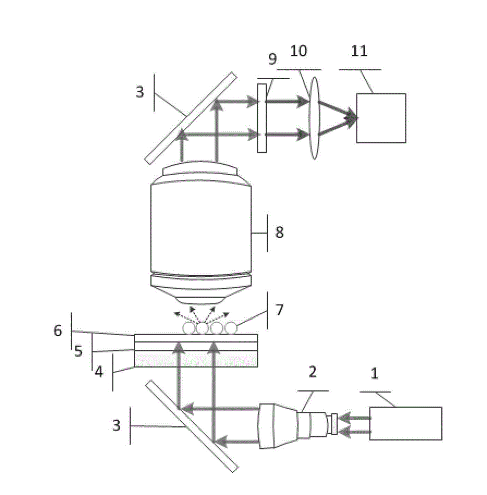
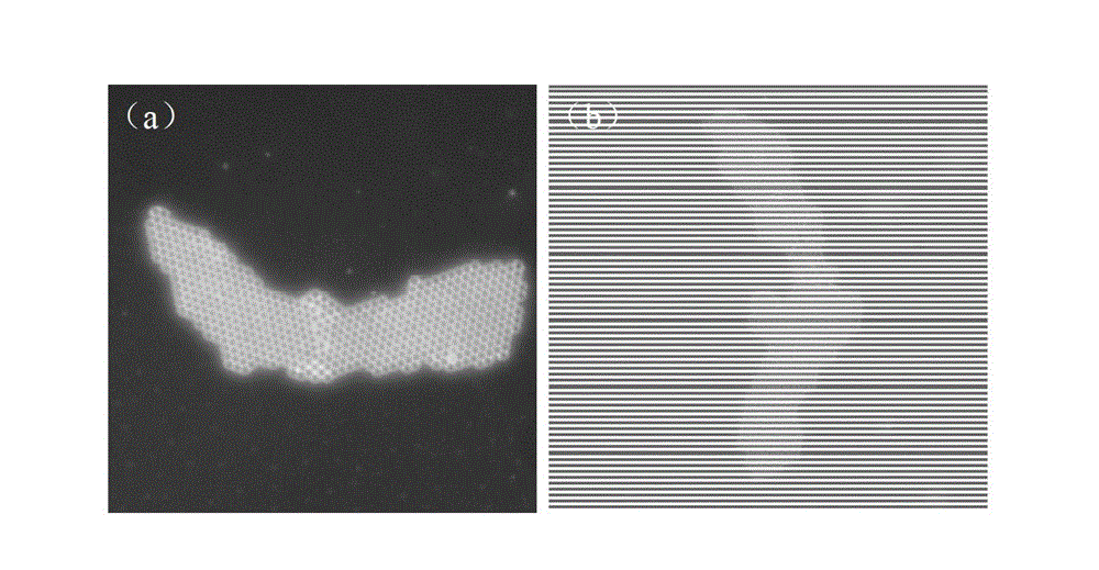
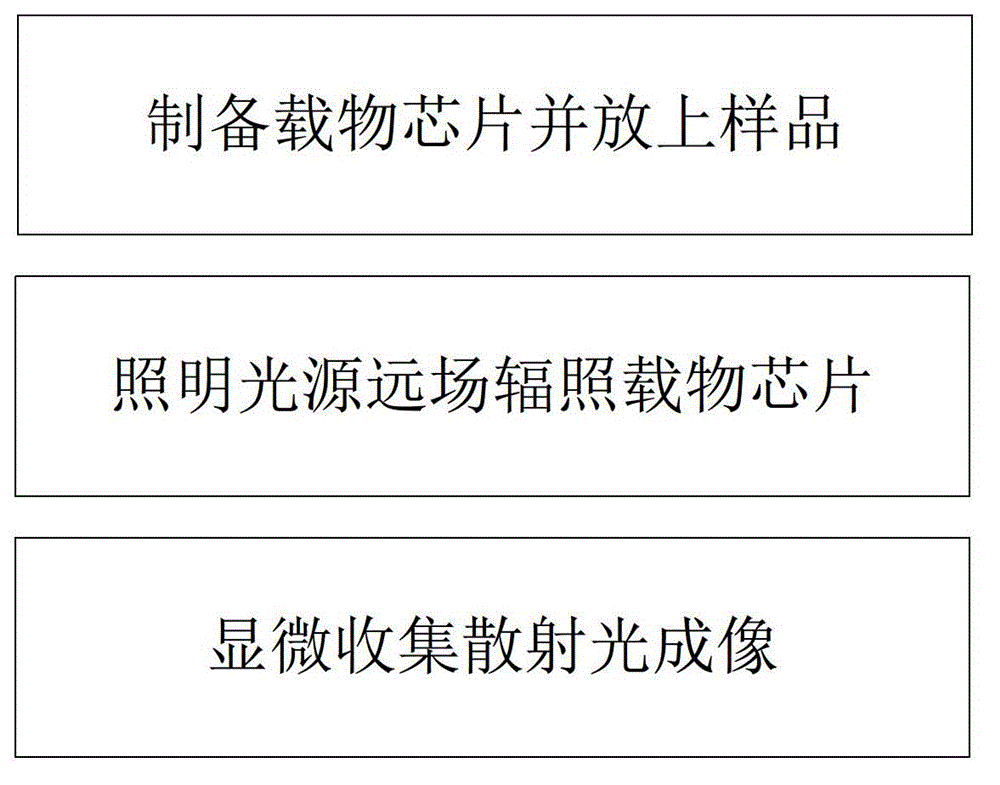
[0024] Such as figure 1 As shown, the present invention is based on waveguide bound fluorescent dark-field microscopy device comprising: illumination laser light source 1, beam expander lens 2, near-end reflector 3, object-loading chip, microscope objective lens 7, far-end reflector 3, filter Sheet 9, collecting lens 10 and CCD image sensor 11. The sample to be observed is placed above the object-carrying chip; the object-carrying chip is composed of a glass substrate layer 4, a metal film layer 5, and a polymer film layer 6 doped with fluorescent molecules from bottom to top, which are used to bind the excited fluorescence and directly Realize the function of dark field; the metal film layer 5 is composed of a layer of silver, and the polymer film layer 6 doped with fluorescent dye is composed of PMMA (polymethyl methacrylate) containing fluorescent molecules; the fluorescent molecules are R6G; the illumination laser The wavelength of light source 1 is 532 nm. The metal thi...


PUM

PropertyMeasurementUnit
Wavelengthaaaaaaaaaa
Thicknessaaaaaaaaaa
Thicknessaaaaaaaaaa

Abstract

The invention discloses a fluorescent dark field microscopy device and method based on waveguide constraint. The fluorescent dark field microscopy device comprises an illumination laser light source, a beam expansion lens, a near-end reflector, a carrier chip, a microobjective, a far-end reflector, a light filter, a collection lens and a CCD (Charge Coupled Device) image sensor; the method comprises the following steps that: the carrier chip which directly realizes the dark field function is prepared; lasers emitted by the illumination laser light source irradiate on a polymer film in the carrier chip through the near-end reflector after being subjected to beam expansion; fluorescence light emitted from fluorescent molecules in the light source forms a guiding mode in the carrier chip and is constrained at an interface of the polymer film and air, and thus, the bottom of a sample nearby the carrier chip is lightened by a near field and scattered; then, light is collected by the microobjective, after the illumination lasers are filtered by the far-end reflector and the light filter, the light is collected by the collection lens and forms an image at the CCD image sensor. The device and the method are based on the constraint of a fluorescent waveguide mode, the microscopy structure is simplified, and the dark field microscopy function is realized.

Description

technical field [0001] The invention relates to the technical field of microscopic imaging, in particular to a fluorescent dark field microscopic device and method based on waveguide confinement. Background technique [0002] As an essential tool in the field of microscopic imaging, optical microscope has been widely used by people in related fields. It is also divided into bright field microscopes, dark field microscopes, phase contrast microscopes, video microscopes, fluorescence microscopes, polarizing microscopes, confocal microscopes, metallographic microscopes, etc. due to different uses. In particular, in the case of some samples whose refractive index is relatively close to the surrounding environment, the observation results under bright field are not obvious, so dark field microscopy is often used for observation. The principle is generally to use some optical components to obliquely incident the illumination source on the sample at a larger angle (greater than th...

Claims


Application Information

Patent Timeline
IPC IPC(8): G01N21/64
Inventor 张斗国陈漪恺韩璐王向贤王沛明海
Owner UNIV OF SCI & TECH OF CHINA
Why Eureka
Try Eureka