Manufacturing method for electrode of lithium niobate optical waveguide device

A production method, lithium niobate technology, applied in the field of communication, can solve the problems of easy corrosion of metal film, difficulty in ensuring accuracy and repeat consistency, etc., and achieve the effect of good consistency, insensitive peeling end point, and controllable corrosion rate

Active Publication Date: 2013-10-16
GUANGXUN SCI & TECH WUHAN
View PDF3 Cites 10 Cited by
  • Summary
  • Abstract
  • Description
  • Claims
  • Application Information

AI Technical Summary

Problems solved by technology

[0007] Since the patterned electrode and optical waveguide must be overlaid accurately, and the SiO2 masks on both sides of the surface of the lithium niobate optical waveguide have been removed before the electrode pattern is overlaid in the existing technology, it is necessary to specially make an overlay mark on the surface of the substrate. , instead of directly overlaying the electrode pattern and the optical waveguide, it is difficult to guarantee the accuracy and repeatability of the overlay
In addition, due to the use of wet etching method to make electrodes, the plated metal film is required to be easy to corrode, and there are restrictions on the types of metal electrodes. Metals such as Pt are difficult to use wet etching.

Method used


Image

  • Manufacturing method for electrode of lithium niobate optical waveguide device
  • Manufacturing method for electrode of lithium niobate optical waveguide device
  • Manufacturing method for electrode of lithium niobate optical waveguide device

Examples


Embodiment Construction

[0034] In order to better understand the present invention, the implementation manner of the invention will be described in detail below in conjunction with specific examples and accompanying drawings.

[0035] The specific production process of the inventive method is as Figure 4 shown, including the following steps:

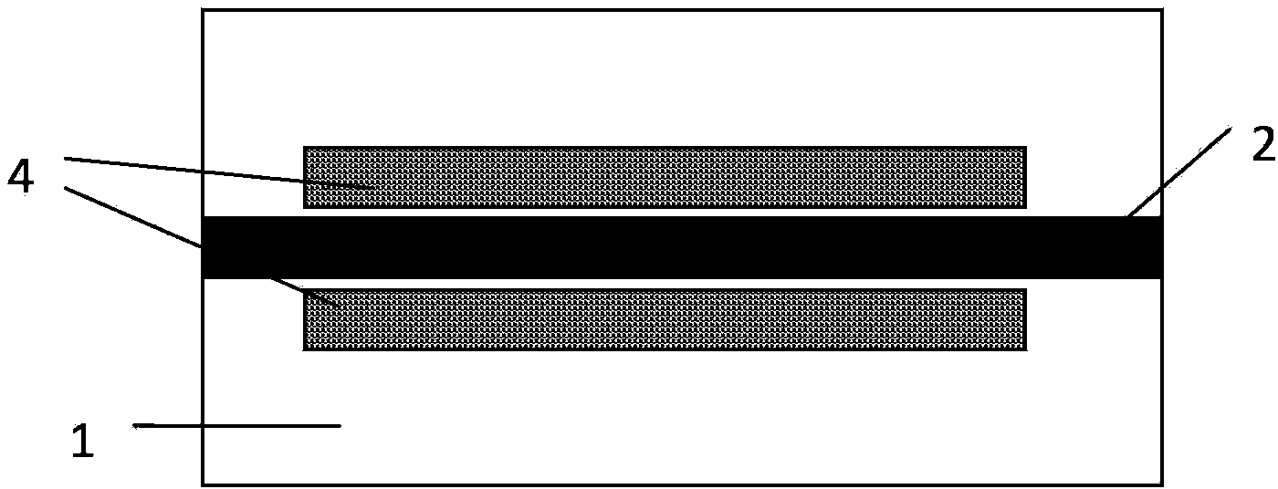
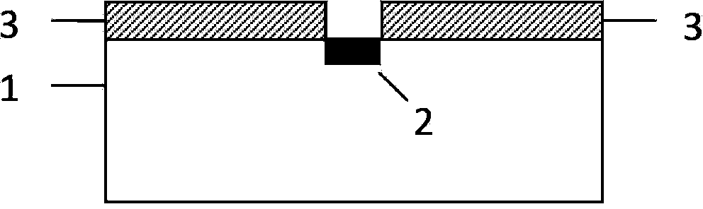
[0036] Step 1: Fabricate an optical waveguide on a lithium niobate substrate: grow a layer of SiO2 film with a thickness of 200nm on the surface of the lithium niobate substrate, and lithographically cut out a SiO2 mask corresponding to the optical waveguide. Using the SiO2 mask, through proton exchange and Subsequent atmosphere annealing technique forms an optical waveguide on the lithium niobate substrate, and the structure of the lithium niobate chip in this step is as follows Figure 3a As shown, it includes a lithium niobate substrate 1 and an optical waveguide 2 formed thereon, and a SiO2 mask layer 3 is provided on the surface of the lithium niobate su...


PUM

PropertyMeasurementUnit
thicknessaaaaaaaaaa

Abstract

Disclosed in the invention is a manufacturing method for an electrode of a lithium niobate optical waveguide device. The manufacturing method comprises the following steps: using SiO2 as a mask and manufacturing an optical waveguide by using annealing proton exchange processing; utilizing the SiO2 mask as a mark to directly carry out self-alignment overlaying on the optical waveguide and an electrode graph; removing the SiO2 mask of the electrode zone by employing a method of combination of dry etching with wet etching; and utilizing sputtering and metal stripping technologies to manufacture the electrode graph and removing the residual SiO2 mask. When the method is used, the electrode graph can be formed at the lithium niobate optical waveguide and accurate overlaying between the optical waveguide and the electrode is ensured; the edge of the electrode is smooth; the defects are less; and the yield is high.

Description

[0001] technical field [0002] The invention relates to a manufacturing method of an optical passive device, in particular to a manufacturing method of an electrode of a lithium niobate optical waveguide device, and the invention belongs to the field of communication. [0003] Background technique [0004] Since the first observation of the optical waveguide phenomenon in the 1960s, the theory of optical waveguides has developed rapidly, and various photonic devices have come out one after another, and have been tried to be applied to many fields. Not only single-function integrated devices such as semiconductor lasers, detectors, optical modulators, optical switches, optical amplifiers, and optical sensors have been produced, but also multiple core devices can be integrated to form a device system with certain complex functions. [0005] Due to its excellent electro-optic, acousto-optic, photoelastic, nonlinear, photorefractive and other properties, lithium niobate crysta...

Claims


Application Information

Patent Timeline
Patent Type & Authority Applications(China)
IPC IPC(8): G02B6/13G02B6/136G02B6/122G02F1/035G03F7/20
Inventor 王定理傅力李林松张登巍吕军
Owner GUANGXUN SCI & TECH WUHAN
Why Eureka
Try Eureka