Semiconductor structure for testing an MIM (Metal-Insulating medium-Metal) capacitor

A semiconductor and capacitor technology, which is applied in the field of semiconductor structure testing of MIM capacitors, can solve the problems of difficulty in determining the relative position and detection of leakage regions in MIM capacitors, and achieves the effects of low cost, simple preparation and improved efficiency.

Active Publication Date: 2013-10-23
SHANGHAI HUALI MICROELECTRONICS CORP
View PDF12 Cites 12 Cited by
  • Summary
  • Abstract
  • Description
  • Claims
  • Application Information

AI Technical Summary

Problems solved by technology

[0006] On the one hand, according to the traditional MIM capacitor design, the entire MIM capacitor is basically surrounded by the insulating medium, even if the insulating medium between the upper and lower plates has a leakage area, but because there is no leakage path to the substrate, the voltage contrast cannot be passed. detected, making it difficult to determine the relative location of leakage regions in bulk MIM capacitors
On the other hand, if the method of peeling off the upper plate of the MIM capacitor layer by layer, and then using the voltage contrast to observe the upper plate to confirm whether there is a leakage path to the substrate, for ordinary MIM capacitor breakdown , the abnormality of the MIM area can be basically observed, but it is powerless for the case of a small degree of leakage

Method used


Image

  • Semiconductor structure for testing an MIM (Metal-Insulating medium-Metal) capacitor
  • Semiconductor structure for testing an MIM (Metal-Insulating medium-Metal) capacitor
  • Semiconductor structure for testing an MIM (Metal-Insulating medium-Metal) capacitor

Examples


Embodiment Construction

[0019] The specific embodiment of the present invention will be further described in detail below in conjunction with the accompanying drawings.

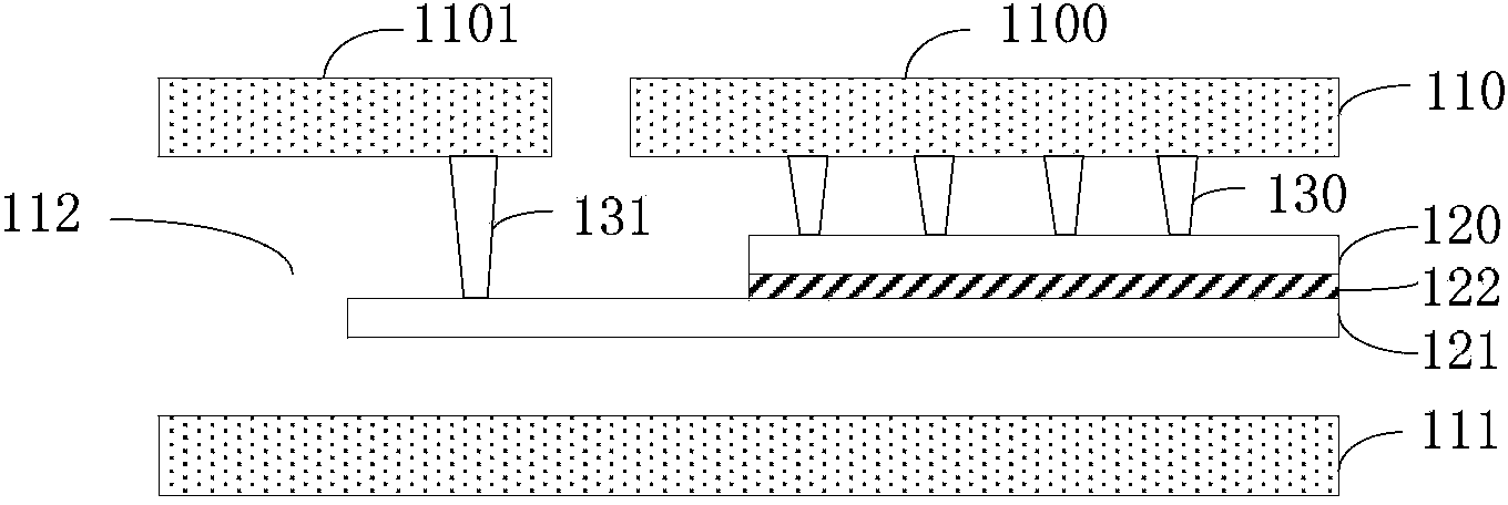
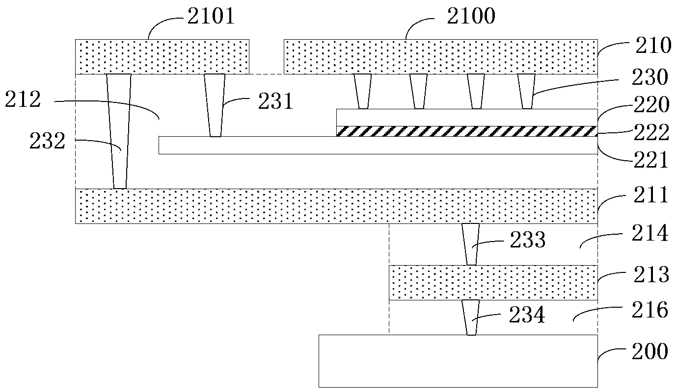
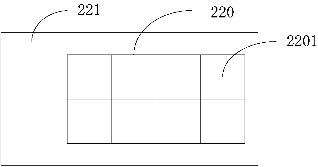
[0020] Such as figure 2 As shown, an embodiment of the present invention provides a semiconductor structure for testing MIM capacitors, including: a first metal layer 210, which can be laid on the surface of the semiconductor structure, or an internal layer of the semiconductor structure, which at least includes The first circuit area 2100 and the second circuit area 2101; the second metal layer 211, which is arranged under the first metal layer 210 with the first dielectric layer 212 as an interval, and a part of the second metal layer 211 is electrically connected to the second circuit area 2101 Connection; the upper pole plate 220 is located in the first dielectric layer 212 at a position close to the first metal layer 210, and the upper pole plate 220 is electrically connected to the first circuit area 2100; the lower pole plat...


PUM


Abstract

A semiconductor structure for testing an MIM (Metal-Insulating medium-Metal) capacitor comprises a plurality of layers, including a first metal layer, a second metal layer, an upper pole-plate and a lower pole-plate; the first metal layer at least comprises a first circuit area and a second circuit area; the second metal layer is arranged under the first metal layer, spaced from the first metal layer through a medium layer and electrically connected with the second circuit area; the upper pole-plate is arranged in the medium layer in a position near the first metal layer and electrically connected with the first circuit area; the lower pole-plate is opposite to the upper pole-plate in the vertical direction, arranged in the medium layer in a position near the second metal layer, spaced from the upper pole-plate through an insulating layer and electrically connected with the second circuit area. The semiconductor structure is formed on a P type semiconductor substrate, and the second metal layer is electrically connected with the P type semiconductor substrate through a first closed circuit, so that a second closed circuit from the upper pole-plate to the P type semiconductor substrate is formed when an electric leakage area exists in the insulating layer; the semiconductor structure can accurately detect whether an electric leakage area exists in the MIM capacitor, is simple to manufacture and low in cost, and is especially suitable for quickly positioning the electric leakage area of a large-area MIM capacitor.

Description

technical field [0001] The invention relates to the field of semiconductor processing and manufacturing, and more specifically relates to a semiconductor structure for testing MIM capacitors. Background technique [0002] The MIM (Metal-Insulator-Metal) capacitor structure is a capacitor structure formed between the interconnection layers of semiconductor devices, which is better compatible with the back-end process of semiconductor manufacturing. Therefore, it is widely used in CMOS processes such as radio frequency integrated circuits and semiconductor memories. [0003] In the MIM capacitor structure defined by two layers of photomasks, its basic structure is distributed from top to bottom as the first metal layer / intermetallic dielectric layer / MIM capacitor upper plate / MIM insulating layer / MIM capacitor lower plate / intermetallic Dielectric layer / second metal layer, where the upper and lower plates can be drawn out through Via (vertical through-hole interconnection techn...

Claims


Application Information

Patent Timeline
Patent Type & Authority Applications(China)
IPC IPC(8): H01L23/544G01R31/26
CPCH01L22/34H01L28/40
Inventor 李强孙转兰杨昌辉
Owner SHANGHAI HUALI MICROELECTRONICS CORP
Why Eureka
Try Eureka