Pure CMOS reference voltage source based on threshold voltage and thermal voltage

A reference voltage source and threshold voltage technology, applied in the direction of adjusting electrical variables, control/regulation systems, instruments, etc., can solve the problems of increased substrate noise coupling, great influence of process deviation, and adverse effects of reference, etc., to reduce Effects of substrate noise coupling, chip area saving, and layout area reduction

Inactive Publication Date: 2013-11-06
UNIV OF ELECTRONIC SCI & TECH OF CHINA
View PDF4 Cites 13 Cited by
  • Summary
  • Abstract
  • Description
  • Claims
  • Application Information

AI Technical Summary

Problems solved by technology

[0004] like figure 1 As shown, the reference "Tien-Yu Lo, Chung-Chih Hung, Mohammed Ismail. CMOS voltage reference based on threshold voltage and thermal voltage, Analog Integr. Circ. Sig. Process, 2010." proposed a pure CMOS reference voltage source, although avoiding the use of V BE Non-linear problems brought about, but still need to use resistors ( figure 1 In the standard digital CMOS process, the resistance needs to be realized by using low-resistance silicide, which not only occupies a large chip area, is greatly affected by process deviation, but also increases the coupling of substrate noise; in addition figure 1 Two op amps are used in the circuit ( figure 1 A0 and A1 in), not only the power consumption will be relatively large, but also the non-ideal factors of the op amp will also adversely affect the reference

Method used


Image

  • Pure CMOS reference voltage source based on threshold voltage and thermal voltage
  • Pure CMOS reference voltage source based on threshold voltage and thermal voltage
  • Pure CMOS reference voltage source based on threshold voltage and thermal voltage

Examples


Embodiment Construction

[0014] The present invention will be further described in detail below in conjunction with the accompanying drawings and specific embodiments.

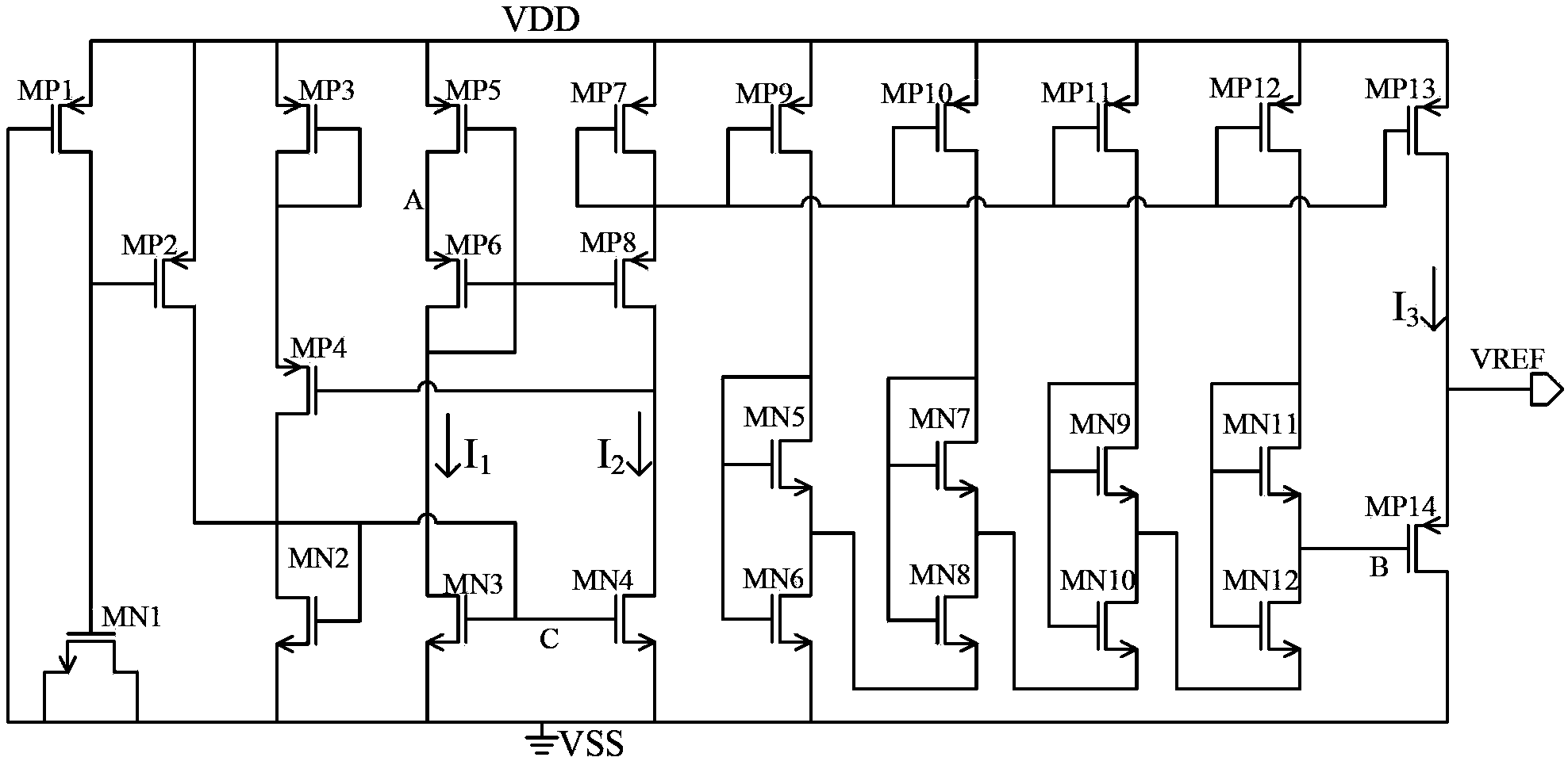
[0015] The present invention is based on the reference voltage source of threshold voltage and thermal voltage, and the specific circuit structure is as figure 2 As shown, it includes: 12 NMOS transistors: MN1~MN12, and 14 PMOS transistors: MP1~MP14. The specific connection relationship is as follows:

[0016] The source terminals of MP1, MP2, MP3, MP5, MP9, MP10, MP11, MP12, and MP13 are connected to the power supply voltage VDD; the gate terminal of MP1, the source and drain terminals of MN1, the source terminal of MN2, the source terminal of MN3, and the The source terminal, the source terminal of MN6, and the drain terminal of MP14 are all connected to the ground potential VSS; the drain terminal of MP1 and the gate terminal of MP2 are connected to the gate terminal of MN1; the gate terminals of MN2, MN3, MN4 and the drain termi...


PUM


Abstract

The invention relates to the field of integrated circuit design, particularly to a pure CMOS (Complementary Metal Oxide Semiconductor) reference voltage source based on threshold voltage and thermal voltage. The invention discloses the pure CMOS reference voltage source based on threshold voltage and thermal voltage and adopts the technical scheme that the pure CMOS reference voltage source based on threshold voltage and thermal voltage comprises 12 NMOS (N-Metal-Oxide-Semiconductor) tubes and 14 PMOS (P-Metal-Oxide-Semiconductor) tubes. The pure CMOS reference voltage source based on threshold voltage and thermal voltage achieves the purpose of reducing the temperature coefficient by utilizing different relationships between threshold voltage and temperature and between thermal voltage and temperature and outputting reference voltage through voltage superposition. The reference voltage source provided by the invention solves the problems of complex structure, higher power consumption, larger territory area, poor CMOS compatibility and the like of the traditional reference voltage source, and rids the traditional reference voltage source of dependence on resistors, bipolar transistors and other devices. The reference voltage source provided by the invention only adopts the MOS tubes, not only is completely compatible with the CMOS technology and saves chip area, but also solves the temperature-dependent nonlinear problem of VBE.

Description

technical field [0001] The invention relates to the field of integrated circuit design, in particular to a pure CMOS reference voltage source based on threshold voltage and thermal voltage. Background technique [0002] As an indispensable unit module circuit in an integrated circuit chip, the reference voltage source has a decisive influence on the performance of the entire system. Usually, the reference voltage determines important system indicators such as the flipping level of the comparator, the oscillation frequency of the oscillator, and the current value flowing in the power tube. It is based on the above situation that the requirements for the reference voltage source circuit continue to increase, and many circuit structures have emerged. [0003] The commonly used reference voltage source is the bandgap reference voltage source using BJT first proposed by Widlar in 1971. It uses the base-emitter voltage of BJT with a negative temperature coefficient and two emitte...

Claims


Application Information

Patent Timeline
IPC IPC(8): G05F1/56
Inventor 周泽坤张其营许天辉苟超崔佳男石跃明鑫张波
Owner UNIV OF ELECTRONIC SCI & TECH OF CHINA
Why Eureka
Try Eureka