Universal detection chip system for weak signals of sensor

A chip system, general detection technology, applied in the direction of using digital measurement technology for measurement, can solve the problems of reducing the reliability of the detection system, occupying a large silicon wafer area, and high cost, achieving miniaturization and portability, and improving integration. accuracy and reliability, and the effect that is conducive to high-precision measurement

Active Publication Date: 2013-11-20
INST OF MICROELECTRONICS CHINESE ACAD OF SCI
View PDF6 Cites 25 Cited by
  • Summary
  • Abstract
  • Description
  • Claims
  • Application Information

AI Technical Summary

Problems solved by technology

There have been foreign reports on the integration of detection microsystems based on CMOS technology and specific sensors [see: Steven M. Martin, Timothy D. Strong, and Richard B. Brown, Design, implementation, and verification of a CMOS-integrated chemical sensor system, Proceeding of the 2004 international conference on MEMS, NANO and smart systems], however, the current range that this system can detect is limited. Since the current-to-voltage conversion uses a transimpedance amplifier, when the current to be measured is very small (below μA level), a large power amplifier above the megohm level is required. Resistors are used to achieve high gain, which will occupy a large amount of silicon area, and at the same time need to compromise between speed and stability, reducing the reliability of the detection system
Moreover, the design and manufacture of single-chip integration methods are difficult and costly. The current research is all for specific sensors, with a narrow detection range and lack of a detection system suitable for a variety of sensors. Therefore, it is necessary to design a sensor with a wide detection range and universal Sensitive sensor weak signal detection chip system

Method used


Image

  • Universal detection chip system for weak signals of sensor
  • Universal detection chip system for weak signals of sensor
  • Universal detection chip system for weak signals of sensor

Examples


Embodiment Construction

[0030]In order to make the object, technical solution and advantages of the present invention clearer, the present invention will be described in further detail below in conjunction with specific embodiments and with reference to the accompanying drawings.

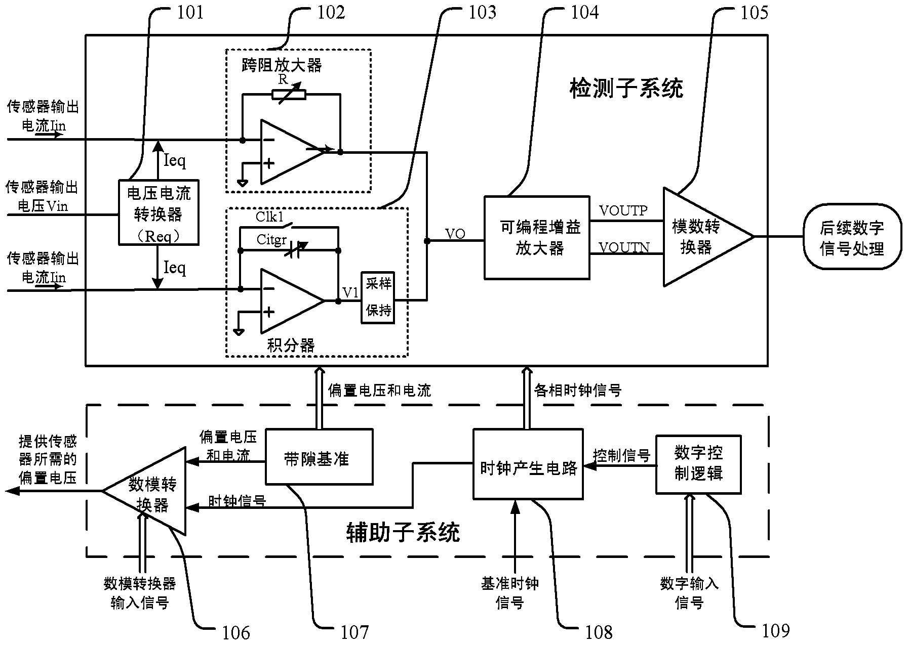
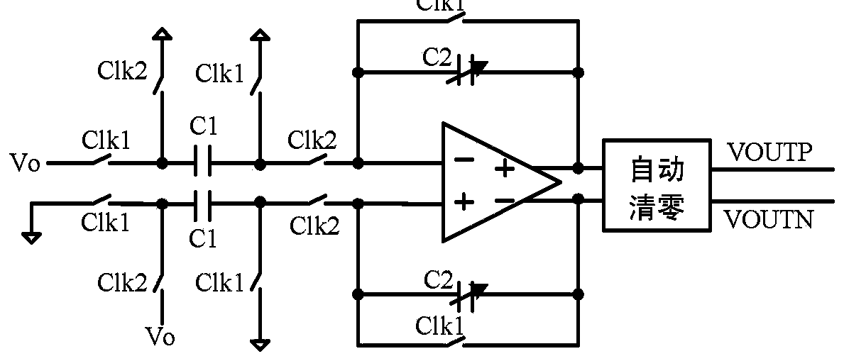
[0031] The sensor weak signal general detection chip system provided by the present invention is such as figure 1 As shown, the chip system includes a detection subsystem and an auxiliary subsystem, both of which are connected to the sensor, wherein: the detection subsystem includes two current detection paths and a voltage detection path, and the current detection path uses current-voltage conversion, voltage amplification and The analog-to-digital conversion realizes the detection of the weak current signal input by the sensor. The voltage detection channel first converts the weak voltage signal input by the sensor into a current signal, and then outputs the current signal to the current detection channel, indirectly real...


PUM


Abstract

The invention discloses a universal detection chip system for weak signals of a sensor. The chip system comprises a detection subsystem and an auxiliary subsystem which are both connected with the sensor, wherein the detection subsystem comprises two current detection channels and a voltage detection channel; the current detection channels realize detection to weak current signals input by the sensor through current and voltage conversion, voltage amplification and analog-digital conversion; the voltage detection channel first converts weak voltage signals input by the sensor into current signals and then outputs the current signals to the current detection channels, thereby indirectly realizing the detection of weak voltage signals; the auxiliary subsystem is used for providing required bias current, voltage, a clock and control signals for the sensor and the detection subsystem. The chip system has the characteristics of low noise, low power consumption, high precision, high integration level and the like, can be integrated on a substrate together with the sensor to form a lab-on-chip.

Description

technical field [0001] The invention relates to the technical field of sensor weak signal detection, and is a general-purpose chip system for sensor weak signals with a relatively large detection range, which can be used to detect weak current signals and weak voltage signals output by various types of sensors. Background technique [0002] Miniature sensors are widely used in environmental monitoring, biomedical engineering, life science research, food manufacturing and processing and other fields. Most of the miniature sensors are ampere sensors or volt sensors, which directly convert chemical or physical quantities into weak current signals or voltage signals. The traditional weak signal detection methods of sensors usually use large instruments such as electrochemical analyzers and lock-in amplifiers. With the development of semiconductor manufacturing technology and the innovation of integrated circuit technology, the design and application of high-performance circuit ...

Claims


Application Information

Patent Timeline
Patent Type & Authority Applications(China)
IPC IPC(8): G01R19/25
Inventor 陈敏刘云涛陈杰
Owner INST OF MICROELECTRONICS CHINESE ACAD OF SCI
Why Eureka
Try Eureka